A final homecoming for a mind that shaped modern chips
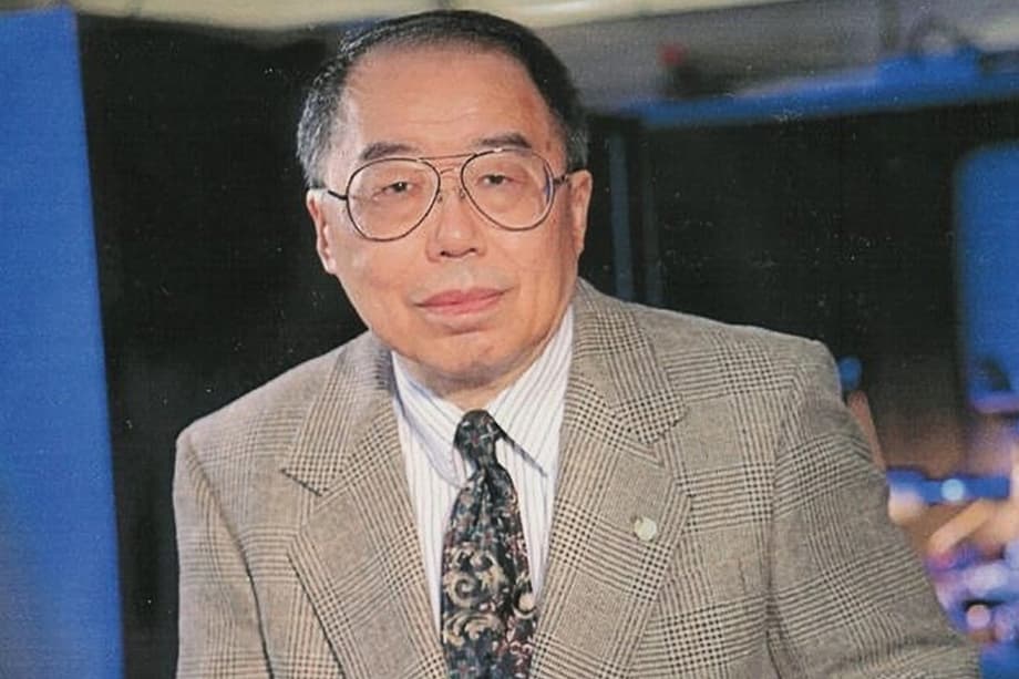
The ashes of Chih-Tang Sah, a pioneer of the modern semiconductor age, have been brought from the United States to Fujian in southeastern China for burial. Sah’s scientific legacy reaches into almost every device with a chip, from the phone in a pocket to the computers that guide aircraft and the accelerators that train artificial intelligence. Working at Fairchild Semiconductor with colleague Frank Wanlass in 1963, Sah co proposed complementary metal oxide semiconductor logic, better known as CMOS. That idea, simple in concept and profound in impact, opened the way to practical low power integrated circuits and the staggering scale of today’s chip industry. By 2011, about 99 percent of semiconductor integrated circuits were produced with CMOS technology, according to the book High-Frequency Integrated Circuits by Sorin Voinigescu of the University of Toronto.
Sah was born in Beijing and passed away on July 5 at the age of 92. He served as an honorary professor at Xiamen University, which marked his death and his long connection to the academic community. The return of his ashes to his ancestral province is a moment to reflect on the science that quietly powers daily life and the global economy, and on a career that bridged laboratories, lecture halls, and the heart of the modern information age.
Who was Chih Tang Sah
Chih-Tang Sah was part of a generation that built the foundations of the information era. Born in China in 1932 and raised in the distinguished Fuzhou Sah family, he pursued engineering in the United States. He earned two bachelor’s degrees at the University of Illinois, then completed his master’s and doctorate at Stanford University. The training placed him at the center of early solid state research just as silicon devices were moving from physics papers into factories.
Education and early career
In 1956, Sah entered industry in solid state electronics and soon joined Fairchild Semiconductor, where he and Frank Wanlass presented the CMOS concept in 1963. The pairing of two types of transistors, one that conducts when the input is high and one that conducts when the input is low, created logic that sipped power at rest and scaled effectively as chips grew more complex. Sah later became a professor at the University of Illinois, serving from 1962 to 1988, and then continued his work at the University of Florida. Across his academic career he published about 280 journal articles, mentored doctoral students, and advanced the device physics that underlies CMOS design and fabrication. He was recognized across industry and academia for contributions that joined theory, devices, and systems.
The University of Illinois Holonyak Micro and Nanotechnology Lab places Sah alongside other giants who shaped the campus legacy of semiconductor research. The lab’s history describes a continuum from the transistor era to modern integrated circuits, with Sah part of that through line. The lab’s historical overview can be found at the Holonyak Micro and Nanotechnology Lab site.
“The lab’s researchers are part of a historic semiconductor legacy that began with engineering giants John Bardeen, Nick Holonyak Jr., and Chih-Tang Sah, whose groundbreaking work helped launch and advance today’s information technology revolution.”
How CMOS changed everything
CMOS, short for complementary metal oxide semiconductor, is the workhorse technology behind most chips. At its heart are complementary pairs of metal oxide semiconductor field effect transistors, or MOSFETs. One type of transistor, called p type, prefers to pass current when the input is low. The other, called n type, prefers to pass current when the input is high. By arranging these as a team for each logic gate, engineers created circuits with very low static power consumption and strong resistance to electrical noise. Current flows significantly only when the circuit switches, which means less heat at rest and better energy efficiency.
Why CMOS uses less power
Consider the simplest logic element, the inverter. In a CMOS inverter, when the input is low, the p type transistor conducts and the n type is off. When the input is high, the n type conducts and the p type is off. For any valid logic level, one device is off, and that limits steady current flow. Power is expended mainly while charging and discharging tiny capacitances during switching. That characteristic led directly to long battery life in portable devices, high density on chips, and a path for designers to keep increasing complexity without a proportional rise in power draw.
CMOS was introduced at Fairchild in 1963 and gained commercial momentum when RCA produced the first CMOS integrated circuits in the late 1960s. By the 1980s it had overtaken other logic families. Today, CMOS sits inside microprocessors, microcontrollers, static RAM, image sensors, and the control logic of countless systems. Even as the physical shape of transistors evolves, with FinFET and gate all around structures replacing earlier planar designs, the logic style remains CMOS. Many modern chips also stack components in three dimensions and use advanced packaging, yet they still rely on the same complementary switching principles that Sah and Wanlass championed.
From Fairchild to the classroom
Fairchild Semiconductor played an outsized role in the growth of Silicon Valley. It gathered scientists and engineers who developed the processes and devices that gave the integrated circuit its early lift. In that environment Sah moved between deep device theory and the practical concerns of manufacturing and design, experience he then brought into the classroom.
Teaching and mentorship
At Illinois, Sah helped cultivate a rigorous understanding of silicon devices and their behavior, strengthening a pipeline of students who would go on to design and build the next generations of chips. The Holonyak Micro and Nanotechnology Lab, which traces its roots to figures like John Bardeen and Nick Holonyak Jr., stands as a living link between that foundational work and current advances. The lab chronicles this lineage in its own history at hmntl.illinois.edu. Academic research and industry collaboration accelerated CMOS from an idea into a near universal platform. A recent perspective in the journal Materials argued that CMOS remains the dominant base for digital systems while new materials and device types are being explored for analog, memory, and neuromorphic computing, provided that they can fit into CMOS compatible manufacturing. That view reflects the maturity and resilience of the platform that Sah helped set in motion.
A legacy seen in phones, planes, and AI accelerators
Evidence of Sah’s influence sits in every pocket and on every desk. The digital logic that executes software instructions, the memory arrays that store data, the sensors that capture images, and the radios that link devices all depend on CMOS techniques. From flight computers in aircraft to control systems in cars and spacecraft, designers choose CMOS for energy efficiency, reliability, and scalability.
Everyday tech built on CMOS
The chips that power cloud services and artificial intelligence also arise from CMOS. Nvidia’s H200 accelerator, one of the most visible products in this category, is built with advanced CMOS process technology. Controls on the export of such high performance chips have become a point of tension between the United States and China. The geopolitics are complex, yet the scientific foundation is simple. The complementary switching that lowers power and enables dense integration, the essence of CMOS, is the common thread across these breakthroughs.
Why this homecoming matters in China today
Returning Sah’s ashes to Fujian carries cultural and scientific symbolism. He was an honorary professor at Xiamen University, and his journey from Beijing to global research labs and classrooms reflects the Chinese scientific diaspora of the past century. China is investing heavily in semiconductor education, research, and manufacturing. The foundational concepts that Sah advanced, such as complementary logic and careful control of device physics, are central to those ambitions.
Export controls, supply chain shifts, and the race to produce smaller, faster, and more energy efficient chips have put semiconductors at the center of national strategies. Yet CMOS is a shared language for engineers. Whether in Beijing, Taipei, Hsinchu, Seoul, Austin, or Dresden, the methods and models that underpin transistor behavior are taught and applied in similar ways. That shared base is part of Sah’s legacy, and it will continue to guide engineers as they reach for new performance and lower power.
The science in simple terms
A MOSFET, the basic device inside CMOS, is a tiny switch that controls current using an electric field. Picture a channel in a semiconductor with source and drain terminals at its ends. A thin insulating oxide separates the channel from a gate electrode. By applying a voltage to the gate, the device attracts or repels charge carriers in the channel. Above a threshold voltage, a conductive path forms and current flows. Below it, the path closes and current stops, aside from tiny leakage.
What a MOSFET does
In CMOS logic, an n type MOSFET pulls an output toward ground when the input is high, and a p type MOSFET pulls the output toward the supply when the input is low. They work in opposition, so only one conducts during steady logic states. That yields near zero static power consumption for logic gates, which is a core reason CMOS became the preferred technology for digital circuits.
Power and scaling
Power in CMOS has two main contributors. Dynamic power comes from charging and discharging capacitances during switching. Leakage power comes from small currents that flow even when transistors are off, which becomes more prominent as devices shrink. Engineers reduce power using circuit techniques such as clock gating, dynamic voltage scaling, and careful layout, and by adopting improved device structures. FinFET and gate all around transistors improve control over the channel, reduce leakage, and support further scaling. Reliability matters too. Designers include protection structures to guard against electrostatic discharge, and they account for stress that can cause metal lines to degrade over time. Beyond digital logic, CMOS supports precision analog functions, image sensing, and radio circuits for 5G and research toward 6G, extending Sah’s influence into nearly every electronic domain.
Final tributes and burial plans
The transport of Sah’s ashes to Fujian brings his life story full circle. He was a scientist of global reach whose work began in China, matured in the United States, and then spread across continents through students, papers, and products. The burial in his ancestral province acknowledges both personal roots and collective gratitude. Xiamen University, where he held an honorary role, stands among the institutions that remember his impact.
From fairchild workbenches to lecture halls and clean rooms across the world, the path of CMOS measures the reach of Sah’s ideas. Every time a device wakes quickly and sips power, there is a trace of his insight. That is a legacy as enduring as the silicon it shaped.
Key Points
- Chih-Tang Sah’s ashes were brought from the United States to Fujian for burial
- At Fairchild in 1963, Sah and Frank Wanlass co proposed the CMOS concept that underpins modern chips
- By 2011, around 99 percent of integrated circuits used CMOS, according to a textbook by Sorin Voinigescu
- Sah taught at the University of Illinois and the University of Florida, publishing roughly 280 papers and mentoring doctoral students
- CMOS enabled energy efficient logic for phones, computers, aerospace systems, and AI accelerators such as Nvidia’s H200
- His return comes amid China’s push to grow its chip sector and ongoing export controls on advanced processors
- Sah was an honorary professor at Xiamen University and is remembered across academia and industry
- Advances like FinFET and gate all around keep the CMOS principle central to new generations of chips