Subsidies power a fast expanding TSMC footprint
Taiwan Semiconductor Manufacturing Co. has secured about NT$147 billion in public support, equal to roughly 4.71 billion US dollars, across a two year period spanning 2024 and the first three quarters of 2025. The funding comes from governments in the United States, Japan, Germany, and China. Company disclosures indicate NT$4.77 billion in subsidies were booked in the third quarter of 2025, taking the total for the first three quarters of 2025 to NT$71.90 billion. Combined with NT$75.16 billion in 2024, the total approaches NT$147 billion.
The support flows through TSMC subsidiaries tied to major projects in each region: TSMC Arizona in the United States, European Semiconductor Manufacturing Company in Dresden, Japan Advanced Semiconductor Manufacturing in Kumamoto, and TSMC Nanjing in China. The funds are largely used for purchases of property, facilities and equipment, and to cover operating costs and other expenses linked to ramping new production sites. Each subsidiary has signed agreements with local authorities that set construction schedules and investment conditions. In Arizona, TSMC is eligible for additional support equal to about 25 percent of certain qualifying investments.
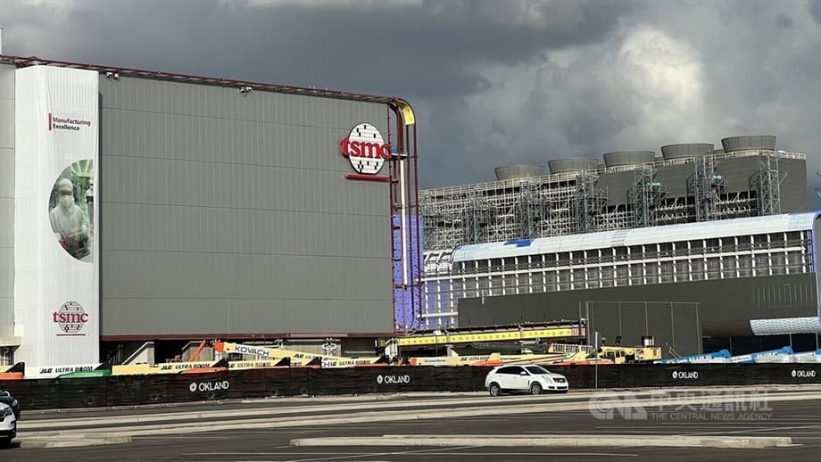
TSMC is investing 65 billion US dollars to build three advanced fabs in Phoenix, with the first fab entering mass production in late 2024. The company has also announced an additional 100 billion US dollars of planned investment in the United States for three more fabs, two advanced packaging facilities, and a major research and development center, lifting its total US commitment to 165 billion US dollars. TSMC describes this as the largest single foreign direct investment in US history and a move that completes a domestic supply chain for advanced AI chips. The company expects large employment gains linked to construction and long term operations. TSMC outlined the expansion plan here: TSMC US investment update.
The push reflects a broader global policy shift. Governments are directing large sums into chipmaking to improve supply chain resilience and to meet surging demand for compute. The US CHIPS and Science Act offers grants, loans, and a 25 percent investment tax credit for eligible semiconductor assets. The EU Chips Act mobilizes tens of billions of euros. Japan has stepped up incentives to attract production. China continues to support domestic manufacturing and downstream data infrastructure. Market demand is the other half of the equation. IDC expects the global semiconductor market to grow by about 15 percent in 2025, driven by AI and high performance computing, with a critical year for 2 nanometer technology and a sharp increase in advanced packaging capacity.
What each country gets from the TSMC buildout
In the United States, the scale of the Arizona expansion is designed to create a complete local ecosystem for advanced logic chips and advanced packaging. TSMC says the enlarged site will support customers that include Apple, Nvidia, AMD, Broadcom, and Qualcomm. The company projects tens of thousands of high paying jobs in chip manufacturing and R&D over time, plus about 40,000 construction jobs across the next four years. The multiplier effects are large. TSMC estimates more than 200 billion US dollars of indirect economic output across Arizona and the wider United States over the next decade as suppliers and service providers build around the fabs. The investment also brings the first TSMC advanced packaging capability to the US, a critical step for AI systems that rely on high bandwidth memory and fast chip to chip interconnects.
Technology and capacity in Arizona
The first Phoenix fab began volume shipments in late 2024, with production centered on advanced nodes targeted by leading US customers. Bringing a new site to full scale requires a careful ramp. Each product must be requalified at the new location to match yield and performance targets. Industry analysts expect the initial capacity of US lines to be lower than in Taiwan as the workforce scales up and as suppliers localize. Experience suggests output and yields rise as teams gain production hours and as the equipment set stabilizes.
Building an ecosystem around Phoenix
Beyond the fabs, the surrounding ecosystem is expanding. TSMC notes it operates a fab in Camas, Washington, and design service centers in Austin and San Jose, which support US based customers. Advanced packaging is also growing in Arizona through multiple projects. Public funding for advanced packaging and test is aimed at shortening product cycles and increasing flexibility for chipmakers and their clients.
Inside JASM in Kumamoto
In Japan, TSMC’s first Kumamoto fab reached commercial production at the end of 2024. A second facility is under construction. The build targets stable supply for Japanese electronics producers and automakers that need reliable access to high quality logic and specialty processes. Japan has broadened its incentives to secure local production and to encourage allied companies to place strategic capacity inside the country. The regional government has supported infrastructure and workforce programs to align with the project’s schedule.
The Kumamoto cluster also serves a policy goal. Japan is working to reduce vulnerability to external shocks while positioning itself in high value parts of the semiconductor chain. Training programs, supplier development, and long term power and water planning are part of that effort. The TSMC presence gives Japan a cornerstone around which smaller suppliers and research institutions can cluster.
Dresden and the Europe push
In Germany, TSMC’s European Semiconductor Manufacturing Company is building a fab in Dresden. The company has stated that mass production timing will depend on client demand and market conditions. The Dresden investment fits with the EU Chips Act and Germany’s strategy to anchor more semiconductor capability in Europe. The region’s automotive and industrial sectors need stable access to logic and mixed signal processes over the long term. Locating capacity near key customers can improve coordination, cut logistics risk, and support localized R&D.
Europe has seen both momentum and setbacks in chip projects. Some high profile efforts have faced delays or cancellations, which highlights the value of firm public private partnerships and realistic build schedules. TSMC’s approach, which ties ramp speed to verified customer demand, reduces the risk of building ahead of the market. As equipment deliveries and workforce pipelines mature, Dresden is positioned to become an important node for European industry.
Nanjing and the China market
In mainland China, TSMC operates a 12 inch fab in Nanjing that introduced the mature 28 nanometer process into production in 2022. The site addresses demand for established nodes that serve automotive, industrial, and consumer applications. TSMC continues to calibrate the site’s operations to global regulations and export controls, which limit the technology nodes available in China. Mature nodes remain central to many products, even as AI drives demand for cutting edge processes elsewhere.
The mature node landscape in China is competitive. Aggressive expansion by local foundries has contributed to oversupply and price pressure, according to industry reports, with spillover effects for producers in Taiwan and other regions. This dynamic pushes foundries to focus on differentiated processes, service quality, and long term customer agreements to defend margins. A balanced global footprint helps TSMC adjust mix and utilization as conditions change.
China is also channeling substantial support into AI infrastructure and domestic chips. Some provinces offer discounted electricity to data centers that deploy domestic processors, which offsets the efficiency gap with restricted foreign devices. The country’s rapid buildout of renewable power and nuclear capacity supplies growing compute demand, although grid constraints and local debt burdens create trade offs. These policies underscore China’s intent to increase self reliance in compute, even at higher short term cost.
Why subsidies matter for cost and capacity
Modern fabs cost tens of billions of dollars and take years to complete. Government support lowers upfront capital requirements and spreads risk that private investors may be reluctant to bear alone. In the United States, a combination of grants, loans, state level incentives, and a 25 percent investment tax credit helps close the cost gap with established hubs. Comparable schemes in Europe and Japan align national priorities with industry needs. The result is a more geographically diverse network that can better withstand shocks.
Experience from 2024 showed that projects without strong financial scaffolding can stall. Equipment lead times, skilled labor availability, and utility upgrades all influence schedules. Public backing for advanced packaging and R&D facilities can unlock bottlenecks in the value chain. Joint venture structures are common, allowing companies to share capital burdens and align product roadmaps. The combination of incentives and partnerships is an efficient route to deliver capacity that supports national strategies for technology and security.
Packaging is a special focus because AI chips require very fast connections between compute die and memory. Advanced methods such as TSMC’s CoWoS and large panel formats are scaling rapidly. IDC expects a sharp increase in production capacity for advanced packaging in 2025. This is essential for top tier AI accelerators and for new server designs that push power and bandwidth limits. Expanding packaging alongside front end fabs improves throughput and reduces logistics risk.
What to watch in 2025 and 2026
Several milestones will show how the TSMC expansion is progressing. Arizona’s second and third fabs, their tooling schedules, and the ramp of advanced packaging will be in focus. The Dresden build will track equipment arrivals and workforce training. In Japan, attention will turn to the second Kumamoto fab’s timeline and its integration with local suppliers. The Nanjing site will remain a bellwether for mature node demand and for the balance TSMC strikes between capacity utilization and pricing.
On the demand side, AI and high performance computing are set to drive orders. Data center operators are increasing spending on accelerators and the memory that feeds them. IDC expects the memory sector to expand faster than the broader chip market next year, with strong growth in high bandwidth memory. Smartphone and PC markets are stabilizing, which supports a recovery in some mature nodes. Automotive electronics continue to grow in value per vehicle, sustaining demand for a range of process technologies.
Policy developments could shape timelines and costs. Final CHIPS Act awards beyond tax credits, state level workforce programs, and permitting reforms influence US projects. The EU and German frameworks will determine how quickly funds reach the Dresden site. Export control changes can affect product mix and cross border logistics. Energy and water planning, especially in arid regions, will remain a constraint to watch as fabs and data centers compete for infrastructure.
Financial posture and market reaction
TSMC’s strong finances give it flexibility to execute these projects. The company increased its third quarter cash dividend by 20 percent to NT$6 per share and approved a capital expansion plan of about 14.98 billion US dollars. Shares have surged this year on optimism around AI demand and advanced node leadership. The rising capital budget aligns with customer preorders and longer term agreements that help underpin fab utilization. Depreciation from new assets will rise, so maintaining high yields and steady volumes is essential to protect margins.
Subsidies reduce the cost of capital for each project and improve the economics of building outside Taiwan. Even with support, local factors such as wages, construction costs, and supplier depth can lift the break even point relative to mature Taiwanese sites. The long life of semiconductor assets means returns are realized over many years. Predictable policy, stable power, and reliable logistics are as important as grants when companies decide where to place their next production line.
Key Points
- TSMC has received about NT$147 billion, or 4.71 billion US dollars, in subsidies from the United States, Japan, Germany, and China across 2024 and the first three quarters of 2025.
- Support is directed to four sites: Arizona, Dresden, Kumamoto, and Nanjing, and is used for equipment, facilities, and operating costs tied to ramping production.
- Arizona anchors TSMC’s largest foreign investment, with a total US plan of 165 billion US dollars for six fabs, advanced packaging, and an R&D center.
- Japan’s first Kumamoto fab began production in late 2024 and a second is under construction, strengthening local supply for electronics and autos.
- TSMC’s Dresden project will time mass production to customer demand, aligning with EU efforts to localize key chip capacity.
- Nanjing focuses on mature nodes, while China’s broader push into mature processes has created oversupply and pricing pressure in that segment.
- AI demand and advanced packaging are central growth drivers in 2025, with IDC forecasting about 15 percent market growth for semiconductors.
- Subsidies, tax credits, and joint ventures help offset higher construction and operating costs outside Taiwan and reduce project risk.