Strategic Upgrade: Japan Enters the 3nm Era
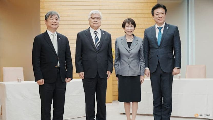
Taiwan Semiconductor Manufacturing Company (TSMC) has officially confirmed plans to manufacture its most advanced 3 nanometre semiconductors in Japan, representing a dramatic upgrade from previous commitments to produce less sophisticated chips at its Kumamoto facility. Chief Executive Officer CC Wei announced the decision during a senior meeting with Japanese Prime Minister Sanae Takaichi in Tokyo, revealing that the company’s second fabrication plant in southern Japan will now target mass production of 3nm chips rather than the originally planned 6 nanometre to 12 nanometre nodes.
- Strategic Upgrade: Japan Enters the 3nm Era
- The $17 Billion Investment Details
- Why 3nm Chips Matter for AI
- Japan’s Government Backing and Economic Security
- The Rapidus Distinction: Complementary Rather Than Competing
- Global Context: Arizona, Taiwan, and Manufacturing Diversification
- Technical Foundations and Local Supply Chains
- Construction Timeline and Regional Impact
- At a Glance
This strategic pivot transforms Japan into the newest location for producing the world’s most sophisticated logic chips, placing the nation alongside Taiwan and the United States in TSMC’s elite tier of manufacturing destinations. The announcement comes as TSMC races to expand global capacity to meet unprecedented demand for artificial intelligence processors, with the company serving as the primary manufacturer for industry leaders including Nvidia.
The $17 Billion Investment Details
Japanese newspaper Yomiuri reported that the upgraded investment will total approximately $17 billion, a substantial increase from the $12.2 billion originally earmarked for the second Kyushu facility. TSMC, while confirming the technological upgrade to 3nm production, declined to verify the specific investment figure. However, the scale of capital commitment signals the project’s critical importance to the company’s global strategy.
Construction of the second fab in Kumamoto has already commenced, with TSMC stating that “the technologies and ramp schedule will be based on our customers’ need and market conditions.” The facility represents a joint venture known as Japan Advanced Semiconductor Manufacturing (JASM), which includes partnerships with Sony and other Japanese stakeholders. During his Tokyo visit, Wei expressed gratitude to the Japanese central government, Kumamoto Prefectural Government, and local communities for their continued support of the ambitious project.
The investment builds upon TSMC’s existing presence in the region, where the company’s first Kumamoto fab began operations in February 2024. That initial facility focuses on producing chips using established process technologies, while the new plant will handle the most advanced 3nm nodes critical for next generation artificial intelligence applications.
Why 3nm Chips Matter for AI
Three nanometre process technology represents the current frontier of semiconductor manufacturing, enabling chip designers to pack billions more transistors into smaller spaces while improving power efficiency and computational performance. These advanced chips serve as the engines powering high performance computing systems and artificial intelligence servers, driving the current technological revolution across industries from autonomous vehicles to cloud data centers.
The difference between 3nm and the previously planned 6nm to 12nm production is substantial. While 6nm chips serve many consumer electronics and automotive applications adequately, 3nm transistors offer significantly greater energy efficiency and processing speed. This makes them essential for training and running large AI models, where computational demands double roughly every few months and power consumption represents a major operational cost.
TSMC currently produces its 3nm chips exclusively in Taiwan, with plans to begin manufacturing at its second Arizona facility in 2027. The addition of Japanese production capacity provides crucial geographic diversification for a supply chain that has faced mounting pressure from geopolitical tensions and the concentration of advanced manufacturing in Taiwan.
During his meeting with Prime Minister Takaichi, Wei emphasized the economic significance of the announcement. The CEO stated:
We believe this fab will further contribute to the local economic growth and, most importantly, form a foundation for Japan’s AI business.
Wei added that TSMC is actively discussing further collaboration with Japanese customers and partners across multiple areas essential to the artificial intelligence industry.
Japan’s Government Backing and Economic Security
The Japanese government has positioned semiconductor manufacturing as a “national project” designed to ensure the country remains strategically essential amid technological competition between major global powers. According to analysis from the Brookings Institution, Japan is investing approximately 0.71% of its gross domestic product (roughly $25.7 billion) between 2022 and 2025 to revive its semiconductor sector, a proportion significantly higher than Germany’s 0.41%, the United States’ 0.21%, or France’s 0.2%.
Tokyo has already provided substantial subsidies to support TSMC’s first facility in Kyushu and is reportedly considering additional financial backing for the upgraded 3nm investment plan. Prime Minister Takaichi emphasized that 3nm chips hold great significance for economic security, reflecting Japan’s broader strategy to secure supply chains for critical industries including electronics, automotive manufacturing, and defense applications.
This government support aligns with a defensive industrial policy aimed at mitigating risks from potential supply chain disruptions. Japan’s Ministry of Economy, Trade and Industry initiated talks to invite TSMC investment back in 2019, before the pandemic highlighted global chip shortages, demonstrating long term strategic foresight regarding the vulnerability of concentrated manufacturing capabilities.
The Rapidus Distinction: Complementary Rather Than Competing
Japan is simultaneously pursuing another ambitious semiconductor initiative through Rapidus, a domestic foundry venture aiming to produce even more advanced 2 nanometre chips in Hokkaido by 2027. The government has determined that the two projects will serve different markets and applications, ensuring they do not compete directly with one another.
While TSMC’s 3nm facility will utilize proven Fin Field Effect Transistor (FinFET) technology for immediate high volume production, Rapidus plans to leapfrog directly to Gate All Around (GAA) architecture for 2nm production. This technological distinction means Rapidus targets a future generation of high performance computing and military applications requiring cutting edge radiation tolerance and energy efficiency, while TSMC’s Kumamoto plant addresses immediate commercial demand for artificial intelligence processors.
The Brookings analysis notes that Japan’s dual track strategy represents a hedging approach, combining the low risk, high certainty TSMC partnership with the high risk, high return Rapidus venture. This diversification allows Japan to rebuild its semiconductor ecosystem through immediate TSMC driven economic activity while maintaining aspirations for future technological leadership through indigenous capabilities.
Global Context: Arizona, Taiwan, and Manufacturing Diversification
TSMC’s Japanese expansion occurs within the context of massive global capacity investments. In March 2025, the company announced its intention to expand United States investment to $165 billion, including three new fabrication plants and two advanced packaging facilities in Arizona. The second Arizona fab is scheduled to begin installing 3nm production tools in the summer of 2026, with volume production targeted for 2027, the same timeframe now envisioned for the upgraded Japanese facility.
The parallel development of 3nm capacity in both Arizona and Kumamoto reflects TSMC’s strategy to create geographic redundancy for its most valuable customers, including Apple, Nvidia, AMD, and Qualcomm. By distributing advanced manufacturing across three distinct political jurisdictions, the company reduces risks associated with regional conflicts, trade disputes, or natural disasters that could disrupt concentrated production in Taiwan.
Market analysts noted immediate investor confidence in the Japanese expansion strategy, with TSMC’s U.S. listed American Depositary Receipts rising 0.77% before market open following the announcement. The investment also strengthens Japan’s position within the global semiconductor supply chain, where domestic companies already dominate critical equipment and materials segments, including an 88% global market share for coater developers and 53% for silicon wafers.
Technical Foundations and Local Supply Chains
The success of TSMC’s Japanese venture relies heavily on the nation’s existing semiconductor infrastructure. Japanese suppliers including Tokyo Electron, Shin Etsu Chemical, and Ibiden provide essential equipment, materials, and packaging substrates required for advanced chip manufacturing. TSMC has reportedly set a target of achieving 60% local procurement for its Kumamoto operations, ensuring that the investment generates broad economic benefits throughout Japan’s industrial base.
This supply chain integration proves crucial for advanced packaging technologies like Chip on Wafer on Substrate (CoWoS), which TSMC uses extensively for artificial intelligence chip production. Companies such as Ajinomoto, traditionally known for food products but now a major producer of Ajinomoto Build Up Film (ABF) resin used in chip packaging, have seen their market values triple due to demand from high performance computing applications.
The concentration of these specialized suppliers in Japan provided a compelling technological rationale for TSMC’s initial investment, beyond the government subsidies alone. As Brookings researchers noted, the business case for co developing next generation CMOS image sensors with Sony offered a specific market opportunity that justified the geographic expansion, while the presence of a major local partner like Sony facilitated navigation of complex regulatory processes.
Construction Timeline and Regional Impact
Physical work on the second Kumamoto facility has already begun, marking a significant milestone after previous reports suggested potential delays. In mid 2025, construction at the site had reportedly slowed as TSMC prioritized its massive Arizona expansion, with CEO Wei initially citing regional traffic concerns as a factor. However, the Japanese government refuted these claims, stating that TSMC had not formally reported infrastructure issues.
With construction now proceeding and the technology node upgraded to 3nm, the facility positions Japan to capture significant value from the artificial intelligence boom. The transition from the original plan to produce 6nm to 12nm chips, suitable for automotive and general computing applications, to the 3nm nodes specifically designed for AI accelerators reflects the rapid evolution of market demand over the past year.
The Kumamoto location offers strategic advantages including proximity to existing semiconductor clusters, relatively low earthquake risk compared to other Japanese regions, and strong governmental support from both prefectural and national authorities. These factors combine to create an environment where TSMC can replicate aspects of its Taiwanese operational excellence while satisfying customer demands for manufacturing diversity.
At a Glance
- TSMC confirmed it will manufacture 3nm chips at its second fabrication plant in Kumamoto, Japan, upgrading from previous plans for 6-12nm production
- The investment is reported to reach $17 billion, supported by Japanese government subsidies aimed at economic security
- CEO CC Wei announced the decision during a meeting with Prime Minister Sanae Takaichi in Tokyo, emphasizing the facility’s role in establishing Japan’s AI business foundation
- The facility addresses soaring global demand for artificial intelligence chips, with TSMC serving as a key supplier to companies including Nvidia
- Construction has already begun on the second fab, which joins an existing TSMC facility that opened in Kumamoto in February 2024
- Japan is simultaneously supporting homegrown foundry Rapidus for 2nm production in Hokkaido, with the government determining the two projects will serve different markets without direct competition
- TSMC also plans 3nm production at its second Arizona fab starting in 2027, creating geographic diversification for advanced chip manufacturing beyond Taiwan