A new engine for Malaysia’s chip ambitions
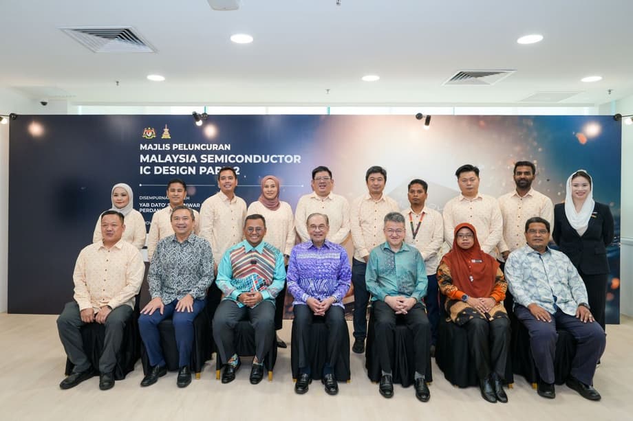
Malaysia has moved to close a critical gap in its semiconductor value chain with the launch of the Advanced Chip Testing Centre at the Malaysia Semiconductor IC Design Park 2 in Cyberjaya. Officiated by Prime Minister Anwar Ibrahim and witnessed by Selangor Menteri Besar Amirudin Shari, the facility is positioned as the first world class chip testing centre in Southeast Asia. It anchors a push to expand beyond contract manufacturing into higher value design, validation, and technology ownership.
The centre ties together the most demanding phases of chip development, from inspection and metrology to emulation, prototyping, validation, and robotics. It is backed by a roster of global technology partners and will operate alongside a new training hub to build the talent pipeline that advanced chip work requires. The vision is straightforward. Reduce reliance on overseas testing, shorten development cycles, and give local chip designers the tools to prove their designs at home.
Cyberjaya was selected for its deep pool of technology companies and research activity. The site, developed with the support of Cyberview Sdn Bhd as the technology hub developer, is designed to encourage collaboration among design houses, equipment makers, software providers, and universities. It also complements the first IC Design Park in Puchong, which already hosts more than a dozen companies and hundreds of engineers. With IC Park 2, Malaysia signals its intent to be a complete hub for chip design through to validation and early production readiness.
What the new centre will actually do
Advanced chips face a long checklist before mass production. Designers must confirm that a chip meets specifications under stress, temperature changes, and electrical noise. They must verify that signals do not degrade at speed, that power delivery stays stable, and that the device can survive the lifetime conditions expected in cars, factories, data centres, and consumer devices. The Advanced Chip Testing Centre brings these steps together under one roof, offering inspection and metrology, design emulation and prototype build, and full validation with automated handling and robotics.
Inside the labs
The inspection and metrology unit focuses on precision measurement of features and materials at micro and nano scale, essential to catch subtle defects that can reduce yield or cause failures in the field. The design, emulation and prototype unit lets teams run complex simulations, map chip behaviour, and build working prototypes for early testing. The validation and robotics unit enables automated, repeatable test routines, from reliability and burn in to system level test, the step where chips are tested in conditions closer to real products. A dedicated research and training unit supports method development, tool calibration, and upskilling for engineers who will run and interpret these tests.
Real world use cases
Use cases range from AI accelerators that run at high power density to automotive microcontrollers that must meet strict quality standards. Testing locally can shave weeks from development by avoiding overseas shipping queues and by allowing rapid rework cycles between design and validation. For startups and new design teams, access to the centre lowers barriers to entry by providing expensive tools as shared infrastructure.
Who is involved and what they bring
The centre is a collaboration between public and private partners. International and local players include Arm, Synopsys, AWS, Keysight, Ansys, Cadence, Sicada, QES, Tekmark, DF Automation, IIT Madras, and the Shenzhen Xinhou Research Centre. Their roles span chip architecture IP (Arm), electronic design automation and verification software (Synopsys and Cadence), multiphysics simulation (Ansys), cloud computing (AWS), test and measurement instrumentation (Keysight), equipment distribution and services (QES and Tekmark), robotics and automation (DF Automation), and academic research and talent development (IIT Madras and Shenzhen Xinhou).
From Puchong to Cyberjaya
IC Park 2 builds on the first IC Design Park in Puchong, where 14 companies employ more than 200 engineers and count on shared services and training to speed up projects. Seven companies based there have advanced workstreams tied to Arm architecture and open design tokens, part of an effort that aims to see Malaysia produce its first locally designed chip as early as 2027 or 2028. The new Cyberjaya site expands the model by adding larger research space, deeper testing capability, and the Advanced Chip Testing Centre as a shared backbone for validation.
Training the next generation
The Advanced Semiconductor Malaysia Academy, housed at IC Park 2, targets the production of 20,000 semiconductor engineers over the next decade. The launch event marked the graduation of seven training cohorts, a sign that the talent pipeline is already flowing. The academy focuses on industry grade skills in design, verification, test engineering, and lab operations, with practical modules built around the tools and workflows used by partner companies.
Prime Minister Anwar Ibrahim framed the talent challenge bluntly during the launch, stressing that infrastructure and incentives mean little without capable local teams ready to deliver for investors and employers.
We can prepare infrastructure and provide incentives, but the most challenging part is the talent pool. What is the point of having infrastructure, good policies, amenities, and incentives if all the workers come from overseas? We also need a well equipped, trained talent pool to protect the interests of this nation.
He also urged young Malaysians to commit to the field, noting that the pace of change in semiconductors demands constant learning. Universities have been encouraged to align curricula with industry requirements, including new programs in AI and chip design that can move from concept to classroom quickly.
Policy and funding support in Selangor
Selangor is pairing the new testing centre with capital for early stage companies. Through Sidec and Permodalan Negeri Selangor Bhd, and in collaboration with Artem Venture Fund, the state is setting up the Selangor Semiconductor Fund, also known as Ehsan Capital, with a target of more than RM100 million. The fund intends to invest in at least seven high potential local startups in areas such as chip design, verification tools, test solutions, and automation. Capital at this stage can help startups bridge the gap between prototype and first customer shipments, a phase that often requires costly lab time and specialized equipment.
Policy is also being used to ensure that technology growth benefits local firms and workers. A Local Economy Development Policy requires 30 percent local content in every new data centre investment. That can translate into procurement opportunities for Malaysian companies in power systems, cooling, connectivity, construction, and facility management, while aligning with the National Semiconductor Strategy, the New Industrial Master Plan 2030, and the National Energy Transition Roadmap.
Why Cyberjaya, and how it complements Malaysia’s chip map
Cyberjaya offers proximity to federal agencies, universities, and a concentration of technology companies and data centres. This environment supports faster problem solving between design teams, equipment vendors, and regulators. It also gives companies convenient access to talent and an airport one hour away, which matters when customers fly in to qualify tools or audit processes. The first IC Park in Puchong is within driving distance, making it easy for teams to move between design offices and the validation labs at IC Park 2.
The new testing hub complements the manufacturing depth in Penang and Kulim, where Malaysia has built a reputation in back end assembly and test over decades. That footprint continues to grow. Advanced Semiconductor Engineering (ASE) has launched a fifth plant in Penang to scale advanced packaging capability for AI era chips, expanding floor space from roughly 1 million to about 3.4 million square feet and planning to hire 1,500 more employees over the next few years. Packaging and testing are becoming a larger share of chip value as devices get more complex. With a cutting edge validation centre in Cyberjaya and major packaging capacity in Penang, Malaysia is building a fuller chain from design to production support.
Key Points
- Malaysia opened the Advanced Chip Testing Centre at IC Design Park 2 in Cyberjaya, the first world class chip testing facility in Southeast Asia.
- The centre integrates inspection and metrology, design emulation and prototyping, validation with robotics, and research and training.
- Partners include Arm, Synopsys, AWS, Keysight, Ansys, Cadence, Sicada, QES, Tekmark, DF Automation, IIT Madras, and Shenzhen Xinhou Research Centre.
- IC Park 2 expands on the first IC Park in Puchong, which already houses 14 companies and more than 200 engineers.
- The Advanced Semiconductor Malaysia Academy aims to train 20,000 engineers over 10 years, with seven cohorts already graduated.
- Prime Minister Anwar Ibrahim stressed that talent is the most challenging part of building a lasting semiconductor ecosystem.
- Selangor is setting up a RM100 million fund, Ehsan Capital, to back local semiconductor startups.
- A Local Economy Development Policy requires 30 percent local content in new data centre investments, aligned with national industrial and energy strategies.
- Cyberjaya’s testing hub complements major packaging expansions in Penang, including ASE’s new plant focused on advanced packaging for AI era chips.