How a modest breakfast reshaped an island economy
One morning in February 1974, seven officials and engineers sat down at a humble shop in Taipei and shared soy milk and fried dough. The bill came to less than NT$400. Before they left the table, they had aligned on a NT$400 million plan that would reshape Taiwan’s economy. They would import integrated circuit technology, train a vanguard of engineers, and build a demonstration factory. The gamble, now remembered as the RCA Project, seeded a manufacturing base that grew into United Microelectronics Corporation and then Taiwan Semiconductor Manufacturing Company. Fifty years later, chips made in Taiwan power smartphones, data centers, and artificial intelligence systems all over the world.
- How a modest breakfast reshaped an island economy
- Crisis, choices, and a bold bet on chips
- From blueprint to silicon
- ITRI, ERSO, and the cluster effect
- How Morris Chang made foundry a winning model
- Transnational networks, not theft
- Geopolitics and the new rules of trade
- What this origin story still teaches
- What to Know
Taiwan faced a hard choice. The 1973 oil shock strained its export model and drove up costs. Diplomatic setbacks had isolated the island in world politics. Premier Chiang Ching-kuo tasked aides with finding a technology that could lift Taiwan’s growth potential. At the table that day was Pan Wen-yuan, a Chinese American engineer who led work at RCA Laboratories in the United States. He argued for an ambitious pivot from labor intensive assembly to integrated circuits. Economics minister Sun Yun-hsuan backed him, and Executive Yuan secretary general Fei Hua drove the idea forward. The plan would focus on complementary metal oxide semiconductor technology, train a cohort abroad, and bring every step of the process home to Taiwan, not just packaging.
Crisis, choices, and a bold bet on chips
The decision was more than an industrial upgrade. It was a statement that Taiwan would climb the value chain through science and engineering. The government appointed the Industrial Technology Research Institute to oversee the project through its Electronics Research and Service Organization. A Technology Advisory Council of overseas experts was convened to steer technology choices and keep the program aligned with market needs. The group targeted consumer electronics where Taiwan’s manufacturers could sell quickly, and it chose CMOS for its low power draw and reliability. The mandate was clear: acquire full manufacturing capability, learn it, improve it, and spread it through new firms.
Who was at the table?
- Sun Yun-hsuan, minister of economic affairs
- Kao Yu-shu, director general of Transportation and Communications
- Wang Chao-chen, president of ITRI
- Kang Pao-huang, director of Telecommunications Laboratories
- Fei Hua, secretary general of the Executive Yuan
- Fang Hsien-chi, director general of Telecommunications
- Pan Wen-yuan, RCA Laboratories director
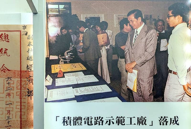
Pan locked himself in the Grand Hotel for ten days to write the plan. In August 1974 it won approval. Critics warned that chips were too capital intensive and too complex. Sun pushed the plan through anyway. Two years later, a contract with RCA enabled technology transfer and in 1976 nineteen engineers left for training in the United States. They returned to Hsinchu and built a demonstration factory designed to teach, not merely to ship product. The message from the top was consistent: this was a national project, and the goal was mastery.
From blueprint to silicon
On October 29, 1977, Taiwan opened its first integrated circuit demonstration plant. It made three inch silicon wafers using a seven micrometer process and aimed at chips for digital watches and consumer devices. The plant was a classroom and a production line. Early setbacks were frequent, but within six months the team raised yields to about 70 percent, surpassing the original RCA line. That single statistic mattered. High yield means more good chips per wafer, lower cost, and a path to profit. The engineers not only learned to run the equipment but also how to improve it in local conditions, a cornerstone of the island’s manufacturing culture.
Why CMOS and seven microns?
CMOS stands for complementary metal oxide semiconductor. It is a way to make transistor pairs that consume very little power when idle. In the 1970s, that trait made CMOS perfect for watches and calculators that ran on tiny batteries. The seven micrometer process refers to the size of features printed on the chip. At the time, seven micrometers was advanced and hard to master. Today top chips are measured in nanometers that are thousands of times smaller, but the methods and discipline that raise yields are timeless: clean rooms, precise lithography, stable chemistry, and rigorous process control.
The demonstration factory produced chips for the island’s first electronic watches. Exports took off. Taiwan quickly became the third largest producer of electronic watches, proof that the new technology could feed real markets. Just as important, a cadre of engineers had built, debugged, and optimized a modern wafer line with their own hands. That talent was about to spin outward.
ITRI, ERSO, and the cluster effect
In 1979, the government established the Hsinchu Science Park to gather research groups, startups, and suppliers near universities and the ITRI campus. The park offered ready land, a streamlined setup process, common utilities, and a community that swapped ideas and solved problems quickly. It was the place where engineers who learned in the demonstration line could form teams, raise capital, and launch companies with close access to tools and mentors. The park became a magnet for returnees from overseas and for multinationals seeking dependable partners.
In 1980, ITRI spun off United Microelectronics Corporation, the island’s first commercial chip firm. It was funded by the state and local banks at the start, then opened to private investors. Alumni from the demonstrative plant went on to found or join new firms in design, testing, and packaging. Companies like Winbond and ASE expanded the ecosystem so that Taiwan did not just make wafers. It designed, tested, assembled, and shipped finished products. That dense network would prove as important as any single champion.
How Morris Chang made foundry a winning model
Despite early success, the next advance required a new business model. In the mid 1980s, ITRI launched a very large scale integration project to prepare for more complex chips. Its new leader, Morris Chang, drew a sharp conclusion from decades in the industry: many design firms wanted to outsource manufacturing to a partner that did nothing else. He proposed a pure play foundry, a factory that would not design its own chips but would build for any client with a design.
In 1987, with Philips investing about 27.5 percent and the government providing a decisive stake, TSMC opened its doors in Hsinchu. The foundry model freed designers from the cost of owning a factory and gave them a technologically neutral partner. It also let TSMC achieve scale by pooling orders across many clients. That scale supported faster process development, tighter cost control, and stronger reliability than most integrated device makers could match. The result was a flywheel: more customers brought more volume, which funded faster process advances, which attracted more customers.
By the early 2020s, TSMC produced the majority of the world’s contract chips and most of the advanced processors behind smartphones, graphics cards, and artificial intelligence servers. It was mass producing three nanometer chips and preparing two nanometer technology. The company’s tight partnership with critical equipment suppliers, including the maker of extreme ultraviolet lithography tools, turned into a strategic advantage. The foundry’s focus on one mission, building for others, reshaped the entire industry.
Transnational networks, not theft
Taiwan’s chip story was built on formal technology transfer contracts, training, and the effort of engineers who tied what they learned abroad to factories at home. It is a tale of collaboration rather than appropriation. The RCA contract was a sale, not a secret. The Technology Advisory Council drew on diaspora expertise to guide choices. The island embedded capability through a demonstration line, then spread it through spinoffs and a science park that welcomed foreign partners. The result is deeply transnational, with designs from California, tools from Europe, and manufacturing discipline honed in Hsinchu.
Two current debates show how that origin still matters. The first is whether advanced manufacturing can be rapidly re created elsewhere. The second is whether Taiwan will give up the strategic value some call a silicon shield. Analysts warn that replicating the island’s cluster takes time, money, and people trained across many specialties.
Honghong Tinn, an assistant professor who studies the history of Taiwan’s technology industries, has described the core economic challenge of rebuilding chip manufacturing in the United States.
Making chips at scale in the U.S. is obviously going to be more expensive, so they would probably need huge subsidies.
Jonas Parello-Plesner, a policy analyst who has studied technology strategy, captured Taipei’s resolve to keep advanced capacity at home.
There is no way Taipei is relinquishing its silicon shield.
Geopolitics and the new rules of trade
Global policy moves have again put Taiwan at the center of chip debates. In 2025, a new round of U.S. tariffs created fresh uncertainty for exporters. Taiwan won temporary relief on semiconductors, but pressure remained on companies to shift some production and to tighten sales controls. Trade friction between the United States and China already had redirected supply chains and investment, with firms moving some final assembly away from the mainland. Taiwan’s firms, which sell to both sides, had to balance resilience, cost, and market access.
China then clarified how it would label chip origin for customs. The new approach defines origin by the location of wafer fabrication, regardless of where a chip is designed or packaged. Because Taipei is treated as domestic by Chinese authorities, chips fabricated in Taiwan are not subject to the punitive tariffs China applies to many U.S. goods. The rule hurts companies that fabricate in the United States and helps foundries in Taiwan and on the mainland. It also underscores how rules about origin can shape the flow of orders toward certain factories.
Even as politics swirls, cross border projects continue. TSMC is building out a manufacturing campus in Arizona. In 2025, Nvidia unveiled its first U.S. made wafer for its Blackwell generation at the site. The wafer still requires advanced packaging, a complex stage that TSMC performs at scale in Taiwan using techniques such as chip on wafer on substrate. A packaging partnership with a U.S. outsourced assembly and test firm is in motion, with operations expected to start in the middle of the decade. This two step flow, wafer fabrication in the United States and advanced packaging in Taiwan, shows how any single plant is only part of a larger chain.
What this origin story still teaches
The breakfast meeting worked because it joined a clear national goal with concrete steps. Leaders chose a specific technology wedge, designed a demonstration line to build competence, and created a park that attracted talent, suppliers, and capital. They trusted engineers with the hardest problems and let new firms carry ideas into markets. Government support at the start did not last forever. Public stakes were sold down as private investors gained confidence, and the industry’s own spending on research rose as it matured.
Today’s challenges remain steep. Advanced chipmaking eats power and water and demands rare skills. Yet the same elements that lifted Taiwan in the 1970s still matter: patient investment, a dense industrial neighborhood, and engineers who learn by building. The legacy of that modest breakfast is not nostalgia. It is a blueprint for how to turn a crisis into a new kind of prosperity.
What to Know
- In 1974, seven leaders agreed to fund a NT$400 million integrated circuit program after a breakfast meeting in Taipei.
- The government chose ITRI and its ERSO unit to run the RCA technology transfer and to train a first wave of nineteen engineers in the United States.
- Taiwan’s first IC demonstration factory opened on October 29, 1977, reached about 70 percent yields within six months, and outperformed the original RCA line.
- Early products included watch chips, which helped make Taiwan the world’s third largest electronic watch exporter.
- Hsinchu Science Park opened in 1979 and UMC spun out of ITRI in 1980, seeding a wider cluster in design, testing, and packaging.
- Morris Chang founded TSMC in 1987 with support from the government and Philips, launching the pure play foundry model that serves fabless chip designers.
- By the early 2020s, TSMC led the global foundry market and produced most of the world’s advanced processors at three nanometers with two nanometers in development.
- New trade rules and tariffs have raised costs and rerouted supply chains, while China’s customs approach favors chips fabricated in Taiwan.
- TSMC’s U.S. expansion is under way, with wafers made in Arizona and advanced packaging still concentrated in Taiwan.
- Taiwan’s success rests on talent, a strong industrial park system, transnational collaboration, and continuous reinvestment in manufacturing excellence.