Why this subsidy matters now
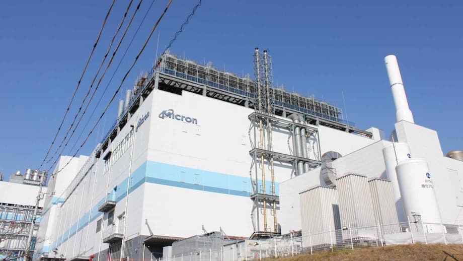
Japan has committed up to 536 billion yen (about 3.63 billion dollars) in support for Micron Technology to accelerate advanced DRAM production at the US companys Hiroshima site. The package, administered by the Ministry of Economy, Trade and Industry, targets both research and development and capital spending and aims to move Micron into volume output of new memory as demand tied to artificial intelligence and data center upgrades grows. Micron plans to begin shipping advanced DRAM from Hiroshima as early as 2028, according to planning timelines shared with industry partners. The award makes Micron one of the largest foreign beneficiaries of Japans semiconductor push, alongside projects to seed advanced logic and packaging in Hokkaido and Kyushu.
How the funding will be used
The support is designed to underwrite a shift to new DRAM production nodes that require extreme ultraviolet lithography equipment, new cleanrooms, and specialized process tools for etch, deposition, inspection, and metrology. This generation of memory, often referred to in industry roadmaps as 1 gamma DRAM, packs more bits into the same area, reduces power consumption, and raises speeds for servers, PCs, smartphones, and advanced vehicles. Japanese suppliers have strengths in photoresists, gases, and precision equipment that will feed into the project, creating second order benefits across the domestic supply network.
Officials have signaled that the government support will offset roughly one third of eligible capital costs, a structure that encourages private co-investment while shortening the payback period on risky long horizon chip projects. Micron has already been preparing its Hiroshima campus for a larger footprint, following earlier government approvals that helped the company bring in EUV tools and update process lines. The new package expands that effort to target true mass production later this decade.
What is advanced DRAM and 1 gamma
DRAM is the short term working memory inside every computing device. It stores data that processors need to access quickly. Progress in DRAM typically comes in steps known as nodes, each step shrinking the features on the chip so that more memory cells fit on a wafer. The 1 gamma node is part of a sequence across the industry that includes 1 alpha and 1 beta. Naming conventions vary by company, and the nanometer labels used in logic chips do not directly apply to DRAM. What matters is that the newer node fits more memory in the same space, with better efficiency and faster input output.
Why EUV matters for memory
EUV lithography uses very short wavelength light to print extremely fine patterns on silicon. Earlier DRAM generations relied on multiple patterning, which required several rounds of lithography and etch to achieve tiny features. EUV replaces some of those steps with a single exposure, which improves pattern fidelity and can reduce defect risk. For DRAM makers, EUV enables smaller cells, tighter spacing, and more reliable patterning of critical layers like wordlines and bitlines. Although EUV tools are expensive and complex to run, they can lower overall cycle time and help unlock the density gains needed at 1 beta and 1 gamma.
Timeline and what to expect from Hiroshima
Micron has mapped out a multiyear schedule for Hiroshima, with site preparation and equipment moves beginning well before the first high volume output. Industry planning indicates construction activity ramping in 2026, followed by installation of core EUV systems and supporting tools. Operations at the new facilities are targeted for around 2027, with initial shipments of advanced DRAM from 2028. That window reflects market realities. The memory business went through a deep downturn in 2023, which forced companies to rebalance cash spending and inventories. The Hiroshima plan is timed to align capacity with the next wave of server and AI demand as cloud operators deploy platforms that require larger memory footprints and faster interfaces.
Products that could emerge from Hiroshima include faster DDR5 for servers and PCs, low power DRAM for mobile devices, and graphics DRAM for accelerators and gaming. DRAM does not replace high bandwidth memory used beside AI accelerators, yet the two categories are linked. AI clusters still rely on large pools of DDR memory in host servers, and graphics processors use specialized DRAM with higher data rates. Raising bit density and lowering power at the base DRAM level is a key ingredient in making large scale AI deployments more efficient.
Japans industrial policy reset
Japan once held more than half of global chip output in the late 1980s. By 2022, the countrys share had fallen to roughly 9 percent as production shifted abroad and investment slowed. The government has since rewritten its approach. Instead of trying to rebuild a closed domestic sector, Tokyo has moved to partner with allied firms and to invest in shared research. This includes the Leading Edge Semiconductor Technology Center that links government, industry, and universities, as well as initiatives that encourage advanced packaging and materials leadership where Japanese companies excel. Policymakers also view a steady supply of sophisticated chips as essential for economic security after pandemic shocks and maritime disruptions exposed the fragility of global logistics.
Economic security lens
The Micron package sits alongside other high profile projects. Rapidus, a new Japanese venture working with partners in the United States and Europe, is targeting 2 nanometer logic production in Hokkaido later this decade. In Kyushu, another cluster is building out logic and packaging capacity to support local manufacturers. These moves aim to diversify supply, reduce reliance on any single region, and deepen cooperation among the United States, Japan, Taiwan, and South Korea. The advanced DRAM site in Hiroshima extends that strategy to memory, which underpins every other computing stack.
Official voices
Economy, Trade and Industry Minister Yasutoshi Nishimura framed the logic behind state support during a 2023 briefing, pointing to the need to keep investing even when the industry cycle is weak and to secure a domestic source of advanced chips for strategic industries.
“The market is rough now, but it is essential that we invest in times like these.”
That view has guided multiple subsidy rounds across memory, logic, and packaging. It also aligns with efforts among allies to widen semiconductor cooperation, harmonize export controls, and share research so that no single chokepoint can disrupt the wider economy.
Jobs, skills and regional impact
Micron inherited a deep engineering base in Japan when it acquired DRAM maker Elpida in 2013. The company now employs more than 4,000 engineers and technicians across the country, with Hiroshima as the core DRAM site. The new phase will support construction jobs, equipment installation, and a broad set of suppliers that provide gas, chemicals, wafer handling, photomasks, and precision parts. Local governments expect spillover effects in training and services as contractors expand to meet cleanroom and utilities needs.
Talent remains a constraint. Japan has a strong pipeline of materials and equipment specialists, yet advanced fab operations require thousands of operators, maintenance experts, process engineers, and software teams. Public programs have been set up to expand semiconductor coursework at universities and technical colleges, while companies add in-house academies to train new hires. Micron and partner firms are likely to lean on both approaches, pairing experienced crews with cohorts of graduates who can grow into tool ownership and process control roles.
Competition and the AI memory race
DRAM is a scale game with a demanding learning curve. Samsung Electronics and SK Hynix are formidable competitors across server, mobile, and graphics memory, and they hold strong positions in high bandwidth memory that powers AI accelerators. Micron has been pushing its own HBM lines while advancing DRAM nodes to improve density and power efficiency. Hiroshima gives Micron a high value production base inside a key market with strong government backing, access to local materials expertise, and a stable rule of law. That combination matters as customers prioritize secure supply chains for infrastructure products that must ship on tight schedules.
The shift to DDR5 in servers is still early, and the transition will run for years as data centers swap older platforms for new. AI workloads need enormous memory bandwidth and capacity, both in accelerators and in host systems. Every watt saved in DRAM cascades through a facilitys power and cooling budget. That is why density gains at 1 beta and 1 gamma nodes, along with improvements in error correction and refresh management, draw intense interest from cloud operators and system makers.
Risks and constraints
Memory is one of the most cyclical corners of the chip industry. Periods of tight capacity can be followed by steep price declines when supply expands faster than demand. Micron and the Japanese government are betting that long run trends in AI, automotive electronics, and cloud services will support sustained DRAM growth, even with swings from year to year. Execution risks remain. EUV tools have long lead times and require precise calibration. Power and water must be scaled to support new cleanrooms. Construction and equipment crews must hit milestones so that qualification can begin on time. Currency moves and interest rates can nudge project budgets in either direction.
Policy variables also matter. Export controls, data rules, and cross border investment reviews shape where companies place tools and how they allocate products. Micron has faced constraints in China, one of the worlds largest memory markets. Diversifying production across the United States, Japan, and other allied economies is one way to manage that exposure. The Hiroshima plan fits this pattern by deepening a base in a country that sits at the heart of the global materials and equipment ecosystem.
What to Know
- Japan will provide up to 536 billion yen (about 3.63 billion dollars) to support Microns advanced DRAM program in Hiroshima.
- The Ministry of Economy, Trade and Industry is channeling funds to both research and development and capital spending.
- Micron targets initial shipments of advanced DRAM from Hiroshima as early as 2028.
- The project is built around EUV lithography and new 1 beta and 1 gamma DRAM nodes that raise density and lower power.
- Earlier approvals in 2023 included up to 192 billion yen to help Micron install EUV equipment in Japan.
- Construction and tool installation are expected to ramp from 2026, with new facilities aiming for operations around 2027.
- Japan is using subsidies, joint research, and alliances to rebuild chip strength after its share fell to about 9 percent of global output by 2022.
- Hiroshima will support thousands of skilled jobs and a wide supplier base in materials, equipment, and services.
- Competitive pressure from Samsung and SK Hynix is intense, as AI drives demand for both DRAM and high bandwidth memory.
- Key risks include industry cyclicality, EUV tool lead times, utilities, talent gaps, and policy shifts in major markets.