What the researchers discovered
A research team in China has captured one of the clearest views yet of what happens to photoresist during the moment that chip patterns are developed. Using cryogenic electron tomography, or cryo-ET, they imaged how dissolved photoresist polymers move, collect, and clump inside the developer liquid at nanometer scale. The images show that a large share of the polymer mass migrates to the gas liquid interface and forms clusters that can drop back onto the wafer and create pattern defects. With that insight in hand, the team found that slightly increasing the post exposure bake temperature and maintaining a continuous developer film over the surface prevents clustering and cuts defect counts on 300 millimeter wafers by more than 99 percent when using deep ultraviolet lithography.
The finding targets one of the most stubborn problems in fabrication. A chip can pass through thousands of steps, and microscopic residues or particles at any stage can create a bridge, a break, or a rough edge that degrades yield. Development is a key step where risk rises, because the exposed resist must dissolve away cleanly and predictably while patterns remain crisp. The new work does not change the basic chemistry of pattern transfer, but it reveals a hidden pathway that explains why some residues appear despite careful process control.
In the experiment, chemically amplified resist polymers were observed in their native liquid environment at resolution better than 5 nanometers. The polymers appeared as flexible, threadlike chains. In films between roughly 25 and 100 nanometers thick, the researchers measured that roughly 80 percent of the polymer mass migrated to the top of the liquid layer, close to where the developer meets air. At that interface the polymers formed weakly entangled clusters that tended to be tens of nanometers across, large enough to create pattern defects if they deposited onto the wafer. Heat could unbind these entanglements, which fits with the observation that a warmer post exposure bake suppressed the clusters.
The group reported two practical levers: raise the post exposure bake from about 95 degrees Celsius to roughly 105 degrees Celsius, and keep a uniform developer film on the surface so that the interface remains controlled and clusters are swept away. In trials on 12 inch wafers with existing resist chemistries and standard deep ultraviolet coat, expose, bake, and develop tools, the combined approach slashed visible residue type defects by more than 99 percent. At the same time, the authors caution that this temperature adjustment is unhelpful for extreme ultraviolet lithography because it spreads acid and blurs the finest features.
How photoresists develop patterns
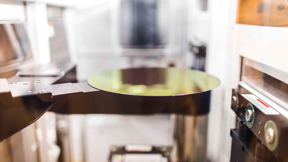
Lithography creates the circuit stencil that shapes every metal and dielectric feature on a chip. A wafer is coated with photoresist, then exposed to patterned light, baked to drive key reactions, developed in a liquid that removes targeted regions, rinsed, and dried. For deep ultraviolet at 193 nanometers and for extreme ultraviolet at 13.5 nanometers, the most common materials are chemically amplified resists. These coatings contain a photoacid generator that releases acid where light strikes. During the post exposure bake, acid catalyzes reactions within the polymer, either making the exposed areas easier to dissolve for positive tone resists or harder to dissolve for negative tone resists.
Development looks simple from the outside, but inside the thin liquid layer the physics and chemistry are complex. The developer dissolves polymer fragments from regions that have been activated by light and post exposure bake. Liquid spreads across the wafer in a controlled puddle or spray pattern, and a very thin film remains while dissolution proceeds. Interfaces matter in this moment. Polymer chains can be attracted to the gas liquid boundary due to surface forces, then entangle and form clusters. If clusters or partially dissolved chains redeposit along an edge or between adjacent lines, they can cause bridging, line breaks, or roughness that appear as defects downstream.
The Chinese team visualized that entanglement directly. The clusters they saw were held together by weak, reversible interactions. That made them sensitive to small changes in temperature and liquid flow history. A warmer post exposure bake increased chain mobility and helped reactions reach completion, which improved dissolution uniformity. A more stable developer film gave clusters less opportunity to form at the gas liquid interface and made it easier to carry away stray chains before rinse and dry.
Why a hotter bake helps DUV but hurts EUV
The same thermal nudge that cleans up residues in deep ultraviolet can undermine pattern fidelity in extreme ultraviolet. In 193 nanometer immersion processes, post exposure bake temperatures around 95 to 110 degrees Celsius are common. Adjusting within that window can improve dissolution contrast, reduce residues, and enlarge the usable process window. The added heat relaxes reversible chain entanglements and accelerates the chemistry that determines which regions dissolve and which remain. Careful tuning is still required, yet increases on the order reported by the researchers are within typical practice for deep ultraviolet track tools and resists.
Extreme ultraviolet patterning is much less tolerant to extra diffusion. The features are smaller and the stochastic variability is higher because the number of absorbed photons per unit area is lower. A small rise in post exposure bake temperature increases acid diffusion length and the movement of other species. That spreads the latent image, softens edges, and raises line edge roughness. It also increases the chance of missing or merged lines at the smallest pitches. For that reason, EUV flows strive to limit diffusion, among other techniques by moderating bake temperature, tailoring quencher content, and switching to materials that do not rely on long range chemical amplification.
Many EUV development programs are moving toward metal containing or metal oxide photoresists with higher EUV absorption and inherently short range reactions. These materials can produce fine patterns with less reliance on acid diffusion. That strategy, combined with dose optimization and improved track processes, aims to hold resolution while suppressing random defects, without resorting to higher bake temperatures that would blur features.
Cryo-ET comes to chipmaking labs
From cells to circuits
Cryo-ET has been a workhorse technique in structural biology. The method traps molecules in a near native state by rapid vitrification, then reconstructs a three dimensional volume from a tilt series of two dimensional electron micrographs. Adapting this approach to semiconductor chemistry required precise timing and sample handling. The research team exposed and baked a wafer in a standard flow, drew off a tiny sample of the developer liquid containing dissolved photoresist chains, then vitrified it within milliseconds on an electron microscopy grid. By rotating the frozen sample inside the electron microscope and collecting many projections, the team reconstructed the three dimensional arrangement of polymers inside the liquid.
The result is a panoramic view of the development step that had previously been out of reach. Traditional tools either examined dried residues, which can change the morphology, or inferred behavior from indirect metrics such as dissolution rate and roughness after the fact. Cryo-ET offers an in situ view. The images in this study showed threadlike chains with random coil shapes, a strong accumulation near the gas liquid surface, and weak entanglements that heating can undo. That evidence supports a straightforward remedy in deep ultraviolet flows: moderate adjustments to bake temperature combined with developer film control on the track.
The team’s data also help explain why leading fabs rarely cite large interface clusters as top defect causes at the very smallest nodes. Killer defects at advanced pitches tend to be smaller than the cluster sizes observed here, which suggests that high end lines already suppress this mechanism through optimized bakes, well controlled track conditions, and advanced rinsing profiles. Cryo-ET gives researchers a sharper diagnostic lens to verify that suppression and to uncover other liquid phase pathways that may matter as dimensions shrink.
What this means for China and the global race
China’s chipmakers are attempting to raise yields while facing limits on access to extreme ultraviolet tools and other advanced equipment. Deep ultraviolet with multiple patterning remains essential for patterning fine features, but each added exposure step multiplies cost and risk. Reports indicate that large foundries in China have pushed older platforms aggressively, which makes defect control and cleaning even more critical for acceptable yield. Any method that reliably reduces development residues with existing tools is valuable in that setting.
The reported recipe is attractive for domestic lines because it does not require a new exposure platform or exotic materials. It uses standard deep ultraviolet resists and track equipment. The proposed changes, a slightly warmer post exposure bake and hardware or recipe tweaks that maintain a stable developer film, are already within common track capabilities. Gains at mature and mid scale nodes could translate directly into more usable chips per wafer.
The same result does not close the gap in extreme ultraviolet patterning. If anything, the study reinforces why EUV success depends on materials that confine reactions and on tightly managed diffusion. Progress there is arriving through new resists, higher power sources, and better metrology, not through higher bake temperatures. The cryo-ET framework still matters because it can clarify liquid phase behavior in many other wet steps that influence final yield.
Limits and what top fabs already do
The study itself points out that the interface clusters it visualized are reversible and relatively large. Leading fabs already avoid leaving bare air liquid interfaces in sensitive windows, and they keep developer films continuous to reduce redeposition risk. Track modules manage puddle formation, dispense rates, and wafer spin profiles to keep both film thickness and residence time in a tight range. Bake plates are calibrated by site across a 300 millimeter wafer. Filters and solution management reduce particulates and dissolved organic carryover.
Modern lithography tracks also embed sensors and in line checks for process drift. Defect pareto analysis and careful design of experiments have steered bake temperatures and developer timings to safe windows for years. What the cryo-ET images provide is a mechanistic picture to match that practical experience. Engineers can confirm that entanglements at the surface are weak, thermal in nature, and responsive to film control. That confidence helps when adding new chemistries or when pushing known recipes to their margins during yield ramps.
Materials on the horizon for EUV
While chemically amplified organic resists still dominate deep ultraviolet lines, the balance in extreme ultraviolet continues to shift toward metal containing systems. Metal oxide and metal cluster resists based on tin, hafnium, zirconium, and related elements absorb more EUV photons per unit thickness. They also form networks upon exposure that do not rely on long range acid transport. Those traits help to reduce line width roughness and support patterning at dimensions below 15 nanometers with doses that remain practical for production tools. Researchers are tuning synthetic routes, including vapor phase infiltration and non aqueous sol gel chemistry, to create uniform, defect resistant coatings with controllable sensitivity.
One recent study blended two tin oxide clusters to achieve both high sensitivity and improved edge etch resistance. The blend produced half pitches in the range of 13 to 16 nanometers at doses around 50 to 60 millijoules per square centimeter, with better etch survival and thicker, more robust patterns. Spectroscopic analysis suggested cooperative interactions between the clusters during exposure and post exposure reactions. Work of this type points to a materials route for sharper EUV images that does not invite the diffusion penalties of higher bake temperatures.
Future projects in this area target ligand design, new metal combinations, and synthesis control to suppress random defect formation while holding resolution. If successful, these materials will reduce the dependence on aggressive bake steps and give track engineers more room to fine tune development without sacrificing edge acuity.
What to watch in manufacturing
For chipmakers running deep ultraviolet, the immediate takeaway is practical. Verify the bake and developer windows with the specific resist on the track and quantify any change in residue defects. Bake uniformity across the wafer, developer puddle timing, and dispense dynamics can all influence whether clusters have time to form and redeposit. The study’s temperature range sits inside what many fabs already use, which simplifies evaluation. Care must be taken to avoid overshoot on temperature or time that could damage resists or shift dimensions out of tolerance.
Inspection and metrology matter as much as recipes. A line that can detect and classify residues early in a yield ramp can adjust quickly. Defect maps, line edge roughness metrics, and rinse optimization go hand in hand with the bake adjustments described here. Despite the limited relevance to EUV, the imaging framework itself is a valuable new tool. Cryo-ET can examine liquid phase interactions in other wet steps such as post develop rinse or selective wet cleans, where tiny molecular aggregates often control whether a process is stable.
Key Points
- Cryo-ET enabled a first direct 3D look at dissolved photoresist polymers inside developer, revealing clustering at the gas liquid interface.
- Raising post exposure bake from about 95 to 105 degrees Celsius and keeping a continuous developer film cut residue type defects on 300 millimeter deep ultraviolet wafers by more than 99 percent.
- The cluster entanglements are weak and reversible with heat, which explains why relatively small thermal changes disrupt them.
- The same temperature rise degrades extreme ultraviolet pattern fidelity by increasing acid diffusion, blurring edges, and raising line edge roughness.
- Leading fabs already tune bake and developer settings to avoid these surface clusters, which is why they are rarely seen as killer defects at the smallest nodes.
- China’s fabs that rely on deep ultraviolet multiple patterning could benefit from the DUV friendly aspects of the study, but EUV access and materials remain the larger hurdle.
- Metal oxide and metal cluster resists for EUV aim to deliver high absorption, strong etch resistance, and short range reactions that limit diffusion without hotter bakes.
- Cryo-ET opens a new diagnostic path to study liquid phase interactions in development, rinse, and wet cleans that shape final yield.