

A second Taylor plant targets the circuitry beneath AI memory
Samsung Electronics plans to manufacture advanced components for artificial intelligence memory at its second chip factory in Taylor, Texas, with mass production scheduled for 2030. The proposed facility would use a 2 nanometer manufacturing process, occupy about 2.7 million square feet and supply the base dies that sit beneath stacks of high bandwidth memory, or HBM.
Contents
- A second Taylor plant targets the circuitry beneath AI memory
- What the Texas factory would make
- Construction milestones stretch to 2030
- Why AMD matters to the proposed expansion
- Why Nvidia is asking suppliers to use TSMC
- NVHBM moves more control circuitry into memory
- Memory demand is growing faster than supply
- The first Taylor factory provides the starting point
- Samsung seeks a stronger foundry business
- Key Points
Industry accounts say customers have reserved the plant's entire planned production capacity, with AMD taking most of the volume. Nvidia is also identified as a prospective customer. Samsung declined to comment on the factory report, and the bookings have not been independently confirmed. The detailed split between customers, contract values and production capacity in wafers has not been disclosed.
The project would give Samsung another route into the growing business of manufacturing the logic circuitry inside AI memory. Its memory division makes the chips that store information, while its foundry division manufactures chips containing processing and control circuits. More demanding HBM designs are bringing those two businesses closer together.
Nvidia's requirements also complicate that opportunity. The AI processor designer has reportedly asked Samsung, SK hynix and Micron to use rival TSMC's manufacturing process for base dies in its customized NVHBM memory. Samsung therefore faces two different commercial paths: making memory with TSMC components for Nvidia, and using its own factories for customers including AMD.
The Texas proposal brings those paths into sharper focus. Samsung could remain a major memory supplier even when another company makes the base die, while seeking more manufacturing revenue from customers that choose its own process.
What the Texas factory would make
HBM combines several memory chips in a vertical stack beside a powerful processor. The arrangement lets large amounts of information travel over short distances, helping AI processors receive the data needed for their calculations. Bandwidth means how much data can move in a given time, rather than how much information the memory can hold.
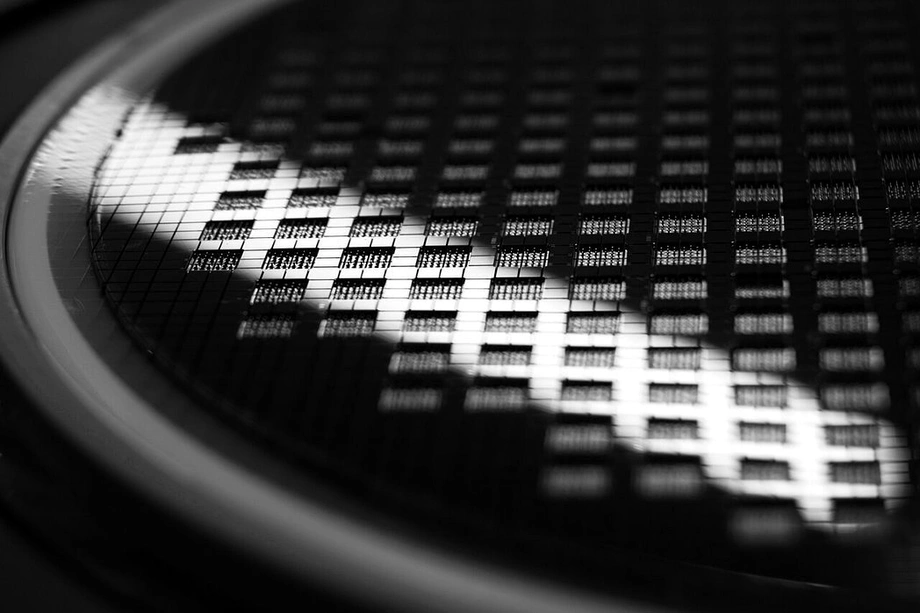
A die is an individual piece of silicon containing electronic circuits. In an HBM stack, the memory core dies store data. The base die underneath them provides connections and logic functions that help the stack communicate with the processor.
Samsung plans to combine base dies manufactured in Taylor with DRAM produced in South Korea. DRAM is the working memory that temporarily holds information while a computing system operates. The proposed production chain would therefore connect American logic manufacturing with Korean memory production.
Samsung's HBM4 products in mass production and its HBM4E samples currently use base dies made with a 4 nanometer process, according to the industry accounts. Taylor Fab 2 would move to 2 nanometers, with the possibility of more advanced processes as future products require them. These process names identify generations of manufacturing technology used to fit increasingly complex circuitry into small chips.
Construction milestones stretch to 2030
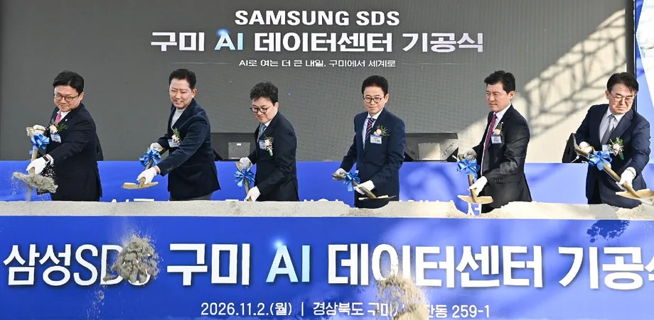
Taylor Fab 2 is planned to cover roughly 250,000 square meters, about 1.5 times the size of the first Taylor factory. Site preparation and ground leveling are reportedly underway, with major construction scheduled to begin in early November 2026.
The timetable separates the start of building work from the installation of manufacturing tools and the eventual production of saleable chips. Chip factories require extensive equipment installation and process preparation after their buildings take shape.
- March 2026: Taylor's city council approved engineering support for permits associated with the second factory.
- Early November 2026: Major construction is scheduled to begin at Taylor Fab 2.
- 2027: The first Taylor factory is expected to begin mass production.
- February 2029: Equipment installation is expected to start at the second factory.
- 2030: Taylor Fab 2 is scheduled to begin mass production.
The schedule puts the second factory several years beyond the immediate scramble for AI memory. Its commercial purpose is to secure a place in later generations of products, when the base die is expected to carry more demanding circuitry.
Why AMD matters to the proposed expansion
AMD accounts for the majority of the reported bookings at Taylor Fab 2. Industry accounts suggest its requirements alone could put pressure on the factory's planned capacity, making the company central to Samsung's proposed expansion.
Samsung intends to keep using its integrated manufacturing model for customized HBM supplied to AMD and other customers. Under that arrangement, Samsung's own businesses would manufacture both the memory core dies and the base dies, rather than purchasing the latter from another foundry.
For Samsung, that approach could bring revenue to both its memory and foundry operations. For AMD, a reservation of manufacturing capacity would provide a place in the production schedule as its AI chip business expands. The precise memory designs covered by the reported Taylor orders have not been described.
The relationship sits alongside a broader effort to improve how processors access data. Samsung presented an AMD memory pooling collaboration during its October 2026 AI infrastructure presentations, together with customized HBM and other memory technologies. The Taylor plan concerns a different part of that effort: manufacturing the silicon underneath future HBM stacks.
Why Nvidia is asking suppliers to use TSMC
Nvidia's reported manufacturing requirement would bring TSMC into a stage of HBM production that Samsung has traditionally handled internally. Industry accounts dated October 18, 2026, say Nvidia asked Samsung, SK hynix and Micron to use TSMC's 3 nanometer process for NVHBM base dies, alongside the sixth generation of DRAM manufacturing technology for the memory core dies.
Nvidia wants memory from its suppliers to behave more consistently. A shared manufacturing process for the base die could reduce differences between products and cut the engineering work required to approve memory from each manufacturer for use with Nvidia processors.
Samsung reportedly accepted the requirement after an internal review. The move extends earlier cooperation with TSMC, which had focused on making Samsung memory compatible with TSMC's chip packaging technology, into the manufacture of an essential HBM component.
The Nvidia base die requirement described in October explains why Samsung's Texas ambitions and its use of TSMC can exist at the same time. Samsung can supply Nvidia with memory that incorporates a TSMC base die while pursuing its own manufacturing orders elsewhere.
NVHBM moves more control circuitry into memory
NVHBM changes the division of work between the main processor and the memory beside it. Its design moves the memory controller, the circuitry that directs data traffic, from the graphics processing unit into the HBM base die.
Nvidia gains space on the main processor for more computing circuitry. The base die takes on a larger role, making its manufacturing technology more important to the complete system. Fitting that additional logic into limited space is one reason for using an advanced process.
Manufacturing yield also affects cost and supply. Yield is the share of chips made on a silicon wafer that meet the required standard. Industry estimates put TSMC's 3 nanometer yield above 90%, compared with roughly 60% for Samsung's 2 nanometer process. Those estimates describe different processes, but they help explain the commercial attraction of a process that can deliver a high proportion of usable chips.
Samsung is also evaluating production of NVHBM base dies using its own manufacturing technology, potentially supplying an alternative if demand exceeds TSMC's capacity. Nvidia's reported preference for TSMC means the proposed Nvidia role at Taylor remains conditional on future sourcing decisions. Conventional HBM and NVHBM could coexist while Nvidia continues selling several generations of processors.
Memory demand is growing faster than supply
UBS forecasts HBM demand of approximately 61.5 billion gigabits in 2027, up 91% from the preceding year. Expected shipments of about 54.6 billion gigabits would leave a gap of 6.9 billion gigabits, or roughly 11% of projected demand.
Those figures measure the amount of memory, rather than the number of finished HBM stacks. The comparison shows why processor companies are seeking capacity commitments well before a new factory starts production.
Nvidia's Vera Rubin production launch adds another immediate source of demand for advanced memory. Samsung, SK hynix and Micron are competing to supply HBM4 for that platform while developing subsequent generations.
Taylor Fab 2's 2030 target comes later than the shortage described in the UBS forecast. The factory would serve a later market, shaped by further growth in AI computing and changes in memory design. Samsung's plan is therefore both a capacity investment and a decision about which parts of future memory systems it wants to manufacture.
The first Taylor factory provides the starting point
Samsung's first Taylor factory is expected to begin production in 2027, three years before the second facility. Tesla is identified as its anchor customer under a reported $16.5 billion agreement covering AI5 and AI6 chips.
The reported investment associated with the first factory has grown from $17 billion to $37 billion, and the project includes $4.75 billion in support under the US CHIPS Act. The wider Taylor site covers 1,268 acres and has room for as many as 10 factories.
The two plants would give the campus different roles. The first is linked to AI processor manufacturing, while the second is being positioned around logic components for advanced memory. For customers, that would expand the range of AI related silicon that Samsung can manufacture in the United States.
South Korea would remain part of the proposed HBM production chain because Samsung plans to make the DRAM there. The Texas expansion would distribute production across the two countries, with American base dies combined with Korean memory.
Samsung seeks a stronger foundry business
Samsung has said its foundry revenue in the third quarter benefited from HBM logic die sales and advanced 2 nanometer orders from large cloud operators and other AI customers. The business nevertheless remained loss making.
The company has projected growth of more than 130% in 2 nanometer orders during 2026. Kiwoom Securities expects the foundry division to return to profit in the fourth quarter. A fully reserved second Taylor factory would support that recovery effort by giving Samsung a longer production pipeline.
Other possible customers remain at an earlier stage. Industry observers identify Broadcom as a potential buyer of Taylor HBM base dies. Samsung is also pursuing a possible 2 nanometer AI chip project for a US cloud customer through Taiwan's Faraday, a company that designs custom chips. Manufacturing orders for that project remain unconfirmed.
AMD's reported demand gives the Texas plan its clearest customer focus. Nvidia presents a more complicated opportunity because its memory requirements currently direct base die manufacturing toward TSMC. Samsung's challenge is to convert demand for its memory into more work for its own factories while meeting each customer's chosen design and production requirements.
Key Points
- Samsung's second Taylor factory is planned to make HBM base dies using a 2 nanometer process, with mass production scheduled for 2030.
- Industry accounts say the entire planned capacity is booked, mostly for AMD. Samsung has not confirmed the report.
- Major construction is scheduled for early November 2026, followed by equipment installation from February 2029.
- Samsung plans to combine Texas base dies with DRAM manufactured in South Korea.
- Nvidia has reportedly asked its three major HBM suppliers to use TSMC's 3 nanometer process for NVHBM base dies.
- UBS projects HBM demand of 61.5 billion gigabits in 2027 against expected shipments of 54.6 billion gigabits.
- The expansion would support Samsung's effort to win more advanced manufacturing business while its foundry division works toward profitability.