
A faster assembly line puts memory supply in focus
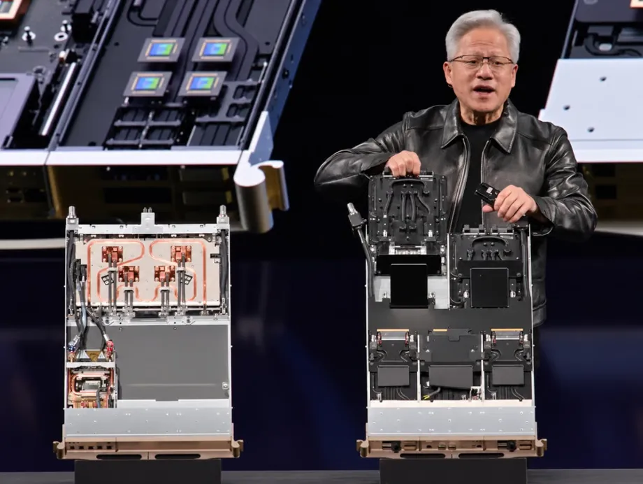
Nvidia has begun full production of its Vera Rubin artificial intelligence computing platform, with chief executive Jensen Huang saying a server node can now be assembled in less than five minutes, compared with two hours for its Grace Blackwell predecessor. The change promises faster server manufacturing while increasing demand for the advanced memory supplied by Samsung Electronics, SK hynix and Micron.
Contents
- A faster assembly line puts memory supply in focus
- What changes inside Vera Rubin?
- Why HBM4 matters to AI performance
- Samsung pursues speed while SK hynix adds capacity
- Micron expands with 2027 capacity already booked
- Packaging and labor can limit deliveries
- HBM4E is already taking shape
- Manufacturers look beyond memory beside the GPU
- The production milestones to watch
- Key Points
Huang presented the Vera Rubin node at GTC Berlin 2026, describing a design without cables or wires and with 100% liquid cooling. Grace Blackwell used liquid cooling for 80% of the system and required considerably more assembly work.
The assembly comparison represents a reduction of more than 95.8%, from 120 minutes to fewer than five. For companies building large numbers of AI servers, simplifying that step could help equipment move through factories faster. The time needed to manufacture chips, package memory and install complete systems remains part of the wider production schedule.
Samsung and SK hynix are competing to capture the resulting demand for HBM4, the sixth generation of high bandwidth memory. Micron is also qualified to supply Vera Rubin, making this a contest among all three major HBM manufacturers.
At the same time, the suppliers are already presenting HBM4E, the next generation after HBM4. Their announcements show two connected pressures: Nvidia wants servers that are easier to build, while memory manufacturers must deliver more speed and capacity through a difficult production process. Faster server assembly makes dependable chip deliveries even more valuable.
What changes inside Vera Rubin?
A server node is a building block of a larger computing system. Nvidia links these units so that many processors can work together on demanding AI tasks, such as training a model or answering requests from large numbers of users.
Vera Rubin's simpler assembly design reduces the work involved in connecting components. Huang's comparison with Grace Blackwell focused on the removal of cables and wires from the node and the move to full liquid cooling.
Liquid cooling carries heat away from components using circulating fluid. Powerful AI processors generate substantial heat, and keeping temperatures under control helps them operate reliably during sustained workloads. Vera Rubin extends that approach across the system described by Huang.
Nvidia's production announcement brings the design into manufacturing. The pace at which finished systems reach customers will also depend on the availability of processors, memory, packaging and cooling equipment.
Why HBM4 matters to AI performance
HBM places several memory chips in a vertical stack beside an AI processor. Tiny connections running through the silicon allow data to move between layers. A shared connecting surface links the stack to the processor, giving it rapid access to information.
AI processors need this access because calculations depend on a constant supply of data. A powerful processor can spend time waiting if its memory cannot deliver information quickly enough. Bandwidth describes how much data can move each second; capacity describes how much can be held at once.
HBM4 widens the data interface to 2,048 bits, twice the width of the previous generation. Samsung reports bandwidth of 2.8 terabytes per second for its stack of 12 layers, while Micron reports more than 2.8 terabytes per second for its current HBM4 product.
Both speed and storage space matter. Training an AI model requires repeated calculations over large amounts of data. Running a trained model, known as inference, also requires memory to hold the model and information about requests being processed.
Samsung pursues speed while SK hynix adds capacity
Samsung's HBM4 combines its sixth generation 1c DRAM manufacturing process with a base die made using a 4 nanometer logic process. The base die is the control layer beneath the memory stack. Samsung reports a data rate of 11.7 gigabits per second at each pin, reaching up to 13 gigabits in optimized configurations.
Hwang Sang-joon, Samsung Electronics' head of memory development, explained the manufacturing choice when the company announced its first commercial shipments:
Instead of taking the conventional path of utilizing existing proven designs, Samsung took the leap and adopted the most advanced nodes like the 1c DRAM and 4nm logic process for HBM4,
SK hynix has taken a different approach with its displayed HBM4 product, using its more established 1b DRAM process and stacking 16 layers. That version holds 48 gigabytes, compared with 36 gigabytes in Samsung's stack of 12 layers.
The SK hynix stack therefore holds 12 gigabytes more, a capacity increase of one third. That extra room can help systems keep more working information close to the processor. Samsung's approach concentrates on faster transfers using a newer manufacturing process.
Long conversations and complex AI tasks make capacity particularly valuable. Models retain information about earlier parts of a request in a temporary store called a key value cache. As more users submit longer requests, that cache can fill available memory and force information into slower storage.
SK hynix development head Ahn Hyeon has forecast that the performance scale required of AI infrastructure could be about 20 times larger in 2030 than in 2026. His argument for new memory technologies rests partly on the growing amount of information that inference systems need to keep readily accessible.
Micron expands with 2027 capacity already booked
Micron opened its second advanced HBM assembly and testing facility in Taichung, Taiwan, in mid October 2026. The plant, known as AATT2, adds capacity for turning individual memory chips into finished stacks.
Manish Bhatia, Micron's president and chief operating officer, described demand at the opening ceremony:
The entire planned 2027 capacity is already sold out,
Micron chief executive Sanjay Mehrotra said at the company's June earnings call that HBM4 had passed $1 billion in cumulative sales within months of commercial shipments starting. He also said production of HBM4 with 12 layers was increasing twice as fast as the equivalent HBM3E production ramp.
Nvidia's Huang confirmed in June that Samsung, SK hynix and Micron had all qualified HBM4 and entered mass production for Vera Rubin. Customer qualification means a supplier's product has passed the checks required for use in the customer's system.
Micron was targeting total HBM production capacity of about 100,000 wafers a month by the end of 2026. Its cumulative investment in Taiwan exceeded NT$1.6 trillion, approximately $50.2 billion, as of June.
The company's Tongluo site in Miaoli County is targeted to begin full product shipments by mid 2027. Wafers from that location would travel about 24 kilometers to AATT2 for assembly and testing, connecting two stages of production within a relatively short distance.
Packaging and labor can limit deliveries
HBM production requires much more than making a working memory chip. Manufacturers must thin the silicon, create precise connections through it and bond multiple layers together. A defect during these steps can reduce the number of usable finished stacks.
Taller stacks increase the number of connections and bonding operations that must succeed. Samsung's choice of a newer process with 12 layers and SK hynix's use of a more established process with 16 layers therefore involve different manufacturing challenges as well as different product specifications.
Equipment supplier Hanmi Semiconductor provides thermal compression bonding machines, which use carefully controlled heat and pressure to join layers. SK hynix signed a contract worth 44.2 billion won, approximately $33 million, in June for upgraded TC Bonder 4.5 Griffin equipment for its Cheongju facility. Hanmi has scheduled its next Wide TC Bonder for commercial release in 2027.
Micron also faces labor uncertainty in Taiwan. Its Taoyuan union reported that 1,994 of 2,012 eligible members authorized strike action on October 7, about 99% of eligible members. Mediation involving the Taichung union was scheduled for October 22. Taiwan President Lai Ching-te attended the AATT2 opening and urged good faith negotiations.
Those developments put attention on staffing as well as factory equipment. The strike authorization was a step allowing industrial action; a walkout and any resulting delivery disruption had not been announced.
HBM4E is already taking shape
Samsung and SK hynix displayed their next generation HBM4E technology at SEDEX 2026, held from October 14 to 16 at COEX in Seoul. Both also displayed Nvidia's Vera Rubin Superchip, showing the close relationship between the memory competition and Nvidia's platform.
Samsung's HBM4E uses 1c DRAM and a base die made with a 4 nanometer process. It reports speeds of up to 16 gigabits per second per pin and bandwidth of 3.6 terabytes per second.
Compared with Samsung's stated HBM4 bandwidth of 2.8 terabytes per second, that is an increase of about 29%. Its HBM4E stack of 12 layers holds 48 gigabytes, one third more than the 36 gigabytes in its HBM4 stack with the same number of layers. Samsung also plans versions with eight layers and 32 gigabytes, and 16 layers and 64 gigabytes.
SK hynix also presented HBM4E with speeds of up to 16 gigabits per second per pin and said energy efficiency would improve by more than 20% compared with HBM4. Samsung supplied samples to customers in May, while SK hynix supplied samples in June for performance checks. Samsung is pursuing mass production in line with customer schedules.
Manufacturers look beyond memory beside the GPU
Samsung displayed a model of zHBM, an architecture that places memory vertically above a computing chip rather than beside it. Shortening the distance between the two could reduce the time and energy spent moving data.
SK hynix presented high bandwidth flash, or HBF, which it expects to offer about 10 times the capacity of existing HBM. The proposed technology would add another level between fast memory and storage, helping AI systems manage larger amounts of data.
Samsung also showed memory capable of performing some calculations internally. That approach aims to reduce how often data must travel to a separate processor. Each proposal addresses a related problem: moving information consumes time and power, even when the computing chip itself is extremely fast.
zHBM and HBF remain at the concept and development stages, with commercialization dates and customer adoption still undecided. For Vera Rubin's current production, HBM4 manufacturing and delivery remain the immediate tasks.
The production milestones to watch
Nvidia's move into full production comes after months of memory qualification, factory expansion and demonstrations of future products. The main milestones show how processor and memory schedules are becoming closely connected:
- Early 2026: Micron's HBM4 entered mass production.
- May and June 2026: Samsung and SK hynix supplied HBM4E samples to customers.
- June 2026: Huang confirmed all three major HBM suppliers were qualified and producing for Vera Rubin.
- October 7, 2026: Micron's Taoyuan union authorized strike action.
- October 14 to 16, 2026: Samsung and SK hynix presented memory technologies at SEDEX in Seoul.
- Mid October 2026: Micron opened its AATT2 packaging and testing facility in Taichung.
- October 22, 2026: Mediation involving Micron's Taichung union was scheduled.
- Mid 2027: Micron targets full product shipments from its expanded Tongluo site.
Samsung and SK hynix stand to gain from Vera Rubin's growing memory requirements, while Micron's contracted capacity shows strong competition for available supply. Customers need complete systems, so rapid node assembly must be matched by sufficient memory, reliable packaging and dependable factory operations.
Key Points
- Nvidia says Vera Rubin is in full production, with node assembly taking less than five minutes instead of two hours.
- The platform uses full liquid cooling and HBM4 supplied by qualified manufacturers Samsung, SK hynix and Micron.
- Samsung's HBM4 stack with 12 layers holds 36 gigabytes; SK hynix's displayed stack with 16 layers holds 48 gigabytes.
- Micron says all planned 2027 capacity at its new Taichung HBM facility is contracted.
- Advanced packaging, equipment availability and labor negotiations remain practical factors in delivery schedules.
- Samsung and SK hynix are testing HBM4E while developing new ways to place and organize AI memory.