
A smaller first phase brings more advanced chips to Japan
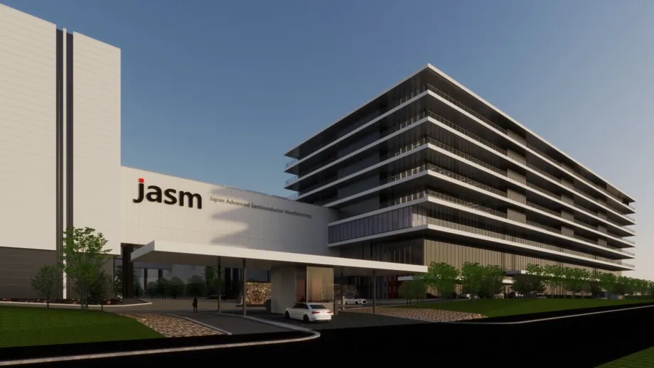
Japan's Ministry of Economy, Trade and Industry approved TSMC's revised Kumamoto factory plan on October 16, 2026, clearing the way for the country's first production of 3 nanometer generation semiconductors. The second factory, under construction in Kikuyo, will initially have capacity for 6,000 wafers a month, with mass production scheduled for December 2028.
Contents
- A smaller first phase brings more advanced chips to Japan
- What 3 nanometer production means
- From February's announcement to December 2028
- Why the subsidy figures have changed
- The first factory gets a narrower role
- Kumamoto's gains come with pressure on daily life
- How Kumamoto fits alongside Rapidus
- The next test is dependable commercial production
- Key Points
The decision changes both the technology and the scale of the project. Taiwan Semiconductor Manufacturing Company, the world's largest contract chipmaker, previously planned monthly capacity of 48,000 wafers using processes from 6 to 12 nanometers, alongside planned production of 40 nanometer chips. The approved first phase instead concentrates on more advanced technology as demand for artificial intelligence computing grows.
Public funding will help determine how far production expands beyond that opening phase. The ministry has reduced the subsidy attached to the current plan to 645.15 billion yen from the previously planned 732 billion yen, while considering an increase in support for the more advanced manufacturing project.
TSMC also secured approval to change its operating first factory next door. That facility will concentrate on 22 and 28 nanometer chips, dropping planned production using 12 and 16 nanometer technology. Together, the revisions give the two factories more distinct manufacturing roles.
For Japan, the approval moves a major industrial investment closer to producing advanced chips domestically. For Kumamoto, it extends a transformation already bringing population growth, traffic congestion and competition for workers. The revised plan leaves the factory site's area and employee numbers unchanged, even as the technology and initial production capacity change.
What 3 nanometer production means
TSMC announced the switch to 3 nanometer technology in February 2026, anticipating rising global demand for AI. The October decision gives government approval to that change and recognizes the revised project as eligible for subsidies.
A nanometer is one billionth of a meter. In chip manufacturing, labels such as 3 nanometers identify a generation of production technology. Modern process names describe a family of manufacturing capabilities rather than a single measurement shared by every feature on a chip.
More advanced processes allow manufacturers to fit greater computing capability into a given area and improve the balance between performance and electricity use. Those qualities matter for demanding applications, including AI computing, where large numbers of calculations must be performed quickly.
A wafer is the thin, round slice of semiconductor material on which many chips are manufactured together. Factories measure capacity in wafers because the number of individual chips produced depends on their size and how many work correctly after manufacturing.
The ministry attributes the reduction in planned wafer output to the shift toward higher performance products. At 6,000 wafers a month, the approved first phase is one eighth of the earlier 48,000 wafer plan for the 6 to 12 nanometer processes. The change combines a more advanced product with a smaller initial manufacturing commitment.
From February's announcement to December 2028
TSMC's February upgrade announcement came during a meeting between chief executive CC Wei and Japanese Prime Minister Sanae Takaichi. The company confirmed the technological change at that stage, while leaving a reported investment estimate unconfirmed.
The main dates now connect that corporate decision with government approval and the planned start of manufacturing:
- Late 2024: TSMC's first Kumamoto factory began mass production.
- February 2026: TSMC announced that the second factory would switch to 3 nanometer technology.
- October 16, 2026: The economy ministry approved revised production plans for both Kumamoto factories.
- Fiscal 2027: The ministry's budget request includes provision for support associated with the revised project.
- December 2028: The second factory is scheduled to begin mass production, with its first shipment planned by that month.
Construction of the second factory is continuing beside the operating first plant in Kikuyo. The ministry's approval covers the second factory's first phase; subsequent expansion will depend on government support and market demand.
Why the subsidy figures have changed
The 732 billion yen figure was the government's earlier planned subsidy for the second factory. Under the revised initial plan, that amount has been reduced to 645.15 billion yen, a decrease of 86.85 billion yen, or about 11.9%.
The smaller initial production commitment is accompanied by a reduction in the investment covered at that stage. At the same time, the move toward mass production using 3 nanometer technology is expected to take investment in the second factory above $15.7 billion, approximately 2.48 trillion yen. The ministry is considering greater assistance in response.
TSMC explained on October 16 that production would be introduced in stages according to market demand and that its planning assumes Japanese government support. The company is therefore linking the pace of expansion to both commercial orders and public financing.
The ministry has included the relevant funding in its fiscal 2027 budget request. A budget request is a proposal for government spending; Japan's budget process determines the money ultimately made available. No final subsidy amount or capacity figure for later expansion has been announced.
The latest investment estimate also follows a larger figure discussed when the upgrade was announced. February coverage put the second factory's possible cost at about $17 billion, a number TSMC declined to confirm at the time. The current expectation is investment above $15.7 billion, while the combined investment in the first and second factories is expected to exceed $23 billion, or 3.5 trillion yen.
The first factory gets a narrower role
TSMC's first Kumamoto factory will focus on 22 and 28 nanometer production under its revised approval. Its earlier plan combined those technologies with 12 and 16 nanometer processes and set monthly capacity at 55,000 wafers.
The new plan removes the 12 and 16 nanometer production and sets capacity at 45,000 wafers a month. That is a reduction of 10,000 wafers, or about 18.2%, from the previous planned total.
The first factory's established production technologies serve applications such as vehicles and industrial equipment. Such products have different requirements from the demanding computing applications associated with the second factory's upgrade. A smaller process number is not the sole consideration when a customer chooses how to manufacture a chip; the product's function, cost and reliability requirements also matter.
Across the two factories, the revised plans separate a larger volume of established technology from a smaller opening phase of advanced production. The first factory will account for 45,000 wafers a month, compared with 6,000 at the second factory's initial stage.
Kumamoto's gains come with pressure on daily life
Kumamoto Governor Takashi Kimura welcomed the approval as an encouraging development for the prefecture. He described the plan's role in the region's recovery in a statement following the decision:
It is encouraging that this will drive a new wave of creative recovery.
The factory upgrade leaves the planned site area and employee numbers unchanged. Residents will nevertheless experience the project within a much wider expansion of semiconductor manufacturing and related businesses around Kikuyo.
The scale of that change was evident in the region's population and traffic pressures before the latest approval. Kikuyo, Koshi and Ozu gained a combined 5,465 residents compared with the 2020 census. Those municipalities also recorded 38 major congestion locations in 2025, about 40% more than in 2021, when TSMC announced its move into Kumamoto.
Kumamoto Prefecture had signed 71 location agreements with semiconductor related companies by the end of March 2026. The agreements show the breadth of corporate interest around the chipmaking project. Five new industrial estates in Kikuyo and nearby municipalities are expected to begin offering plots by fiscal 2031.
Local businesses face a mixed picture. More residents and investment bring demand for meals, accommodation and services, while rising rents, traffic delays and competition for staff increase costs. The decision to manufacture more advanced chips strengthens the region's industrial position, but roads, housing and recruitment remain practical concerns for people already living and working there.
How Kumamoto fits alongside Rapidus
Japan is pursuing advanced chip production through more than one project. Alongside TSMC's Kumamoto expansion, Rapidus is developing 2 nanometer manufacturing in Hokkaido and aims to begin mass production in the second half of fiscal 2027.
Rapidus, established in 2022, has received commitments of roughly $15 billion in Japanese government support. It opened a pilot production line and reached a technical milestone in July 2025, when prototype 2 nanometer transistors demonstrated the expected electrical performance.
Kazuto Suzuki, a professor of science and technology policy at the University of Tokyo's Graduate School of Public Policy and director of the Institute of Geoeconomics, sees the projects as serving different purposes. In his assessment, TSMC's Japanese factories strengthen the country's ability to meet domestic demand, while Rapidus seeks to make Japan an essential supplier of advanced chips to the world.
That difference shapes the customer challenge. Japanese buyers such as Sony, Denso and Toyota have substantial uses for established chip technologies. Rapidus expects to rely heavily on overseas customers for the advanced products it plans to manufacture.
The next test is dependable commercial production
Rapidus illustrates why moving from a technical demonstration to a profitable factory requires more than achieving a smaller process generation. Manufacturers must repeatedly produce large numbers of working chips at a cost customers will pay.
Suzuki identifies production yield, the percentage of manufactured chips that work correctly, as a central measure of success. Explaining how he would judge Japan's semiconductor effort, he said:
If you make a good chip, then that's a success. If you improve the yield, that's a success.
Rapidus has not disclosed its production yield. Chief executive Atsuyoshi Koike has said the company is talking with more than 60 potential customers, and the company announced partnerships with 17 firms on October 5 to help customers design chips. Its planned mass production will test whether technical progress can support regular commercial supply.
TSMC brings extensive contract manufacturing experience to Kumamoto, but its expansion is also being organized around customer demand. The approved 6,000 wafer phase gives the company a defined opening scale for advanced production, with further growth tied to orders and Japanese support.
Japan's immediate milestones are the fiscal 2027 funding process and the second factory's scheduled production start in December 2028. The October approval establishes the technology and the first phase. The next steps will determine how much capacity is built beyond that initial commitment.
Key Points
- Japan approved TSMC's revised Kumamoto plans on October 16, 2026, including the country's first planned 3 nanometer chip production.
- The second factory's approved first phase provides capacity for 6,000 wafers a month, with mass production scheduled for December 2028.
- The subsidy attached to the revised initial plan is 645.15 billion yen, down from 732 billion yen, while additional support is under consideration.
- The first factory will focus on 22 and 28 nanometer chips, with planned monthly capacity of 45,000 wafers.
- Later expansion depends on demand and public support, while Kumamoto continues to manage traffic, housing and labor pressures associated with the investment.