
A bigger investment, with AI memory moving faster
Samsung has raised its planned investment in South Korea's Chungcheong region to 144 trillion won, adding 4 trillion won to the package announced on July 2 and bringing forward the target opening of a major high bandwidth memory packaging plant to June 2028.
Contents
- A bigger investment, with AI memory moving faster
- What the 144 trillion won will fund
- Why packaging matters for AI memory
- Which dates should businesses watch?
- Asan's OLED expansion reaches beyond phones
- Sejong supplies the connections inside AI servers
- Cheonan tests batteries before wider production
- Suppliers and students look for a share of the growth
- Government support now turns to utilities and daily life
- Key Points
The revised plan brings together four affiliates across Asan, Cheonan and Sejong. Samsung Electronics will invest 60 trillion won, Samsung Display 67 trillion won, Samsung Electro-Mechanics 8 trillion won and Samsung SDI 9 trillion won. Their projects cover AI memory, OLED screens, substrates that connect chips to computing systems, and new battery technologies.
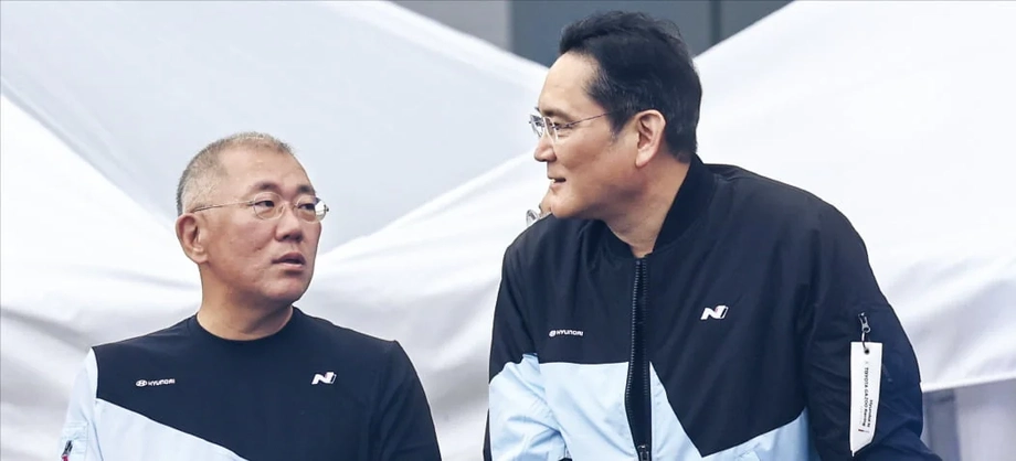
President Lee Jae-myung and Samsung Electronics Chairman Lee Jae-yong attended the November 12, 2026, groundbreaking ceremony at Samsung's Onyang campus in Asan. Foundation work was already under way for Line 5, the new advanced packaging facility intended to help meet growing demand for memory used in AI servers.
Samsung's additional 4 trillion won goes entirely to the electronics affiliate, whose regional commitment rises from 56 trillion won to 60 trillion won. The group's total increases by about 2.9%, while Samsung Electronics' allocation grows by about 7.1%.
The investment also gives Chungcheong a larger role in the less visible stages of semiconductor manufacturing. Making a chip's circuits is only part of the job. Assembling memory stacks, connecting components and testing the finished product are increasingly central to how much useful computing power an AI system can deliver.
What the 144 trillion won will fund
Samsung Display accounts for about 46.5% of the total commitment, making it the largest participant by investment value. Samsung Electronics represents about 41.7%. Together, the two affiliates account for 127 trillion won, or roughly 88.2% of the package.
The allocations are broader commitments covering multiple facilities and stages of expansion. Within them, Samsung has identified several major projects:
- Samsung Electronics: 60 trillion won for HBM facilities and advanced packaging in Onyang and Cheonan, including an initial 6 trillion won for Onyang Line 5.
- Samsung Display: 67 trillion won for Asan and Cheonan, including 5.9 trillion won for the A7 OLED production line.
- Samsung Electro-Mechanics: 8 trillion won for Sejong, including 4.3 trillion won for a new factory making package substrates for AI servers.
- Samsung SDI: 9 trillion won for its Cheonan battery development and production verification base.
Onyang's planned spending extends well beyond the building itself. President Lee said the 6 trillion won packaging facility would be followed by about 40 trillion won in advanced equipment investment. Together, those stages amount to 46 trillion won.
Samsung also plans to expand and modernize HBM equipment at its existing Cheonan site. Linking that operation with Onyang would create a larger production network rather than concentrate the entire memory investment in one new factory.
Why packaging matters for AI memory
HBM places several memory chips in a vertical stack close to a powerful processor. The arrangement lets large amounts of information move over short distances. Bandwidth means how much data can travel in a given time, rather than how much information the memory can store.
AI processors need a steady flow of data to keep working. Faster processors gain less benefit when their memory cannot supply information quickly enough. Advanced packaging helps by making dense, precise connections between memory chips and other components.
Samsung expects Onyang Line 5 to package next generation products, including HBM4E, described as the seventh generation of HBM. Its cleanroom is planned to extend across three floors and cover about 9,400 pyeong, approximately 31,000 square meters. A cleanroom tightly controls dust and other contamination that can damage delicate electronic components.
Lee Jae-yong described the intended change in the site's role during his welcoming address:
"This place, which was centered on simple assembly and testing of conventional chips, will be transformed into a cutting-edge HBM base that is the heart of AI semiconductors," he said.
Samsung's expansion follows its reported Texas base die plans, which envisage manufacturing the circuitry beneath HBM stacks at a second Taylor factory from 2030. The Chungcheong projects focus on the packaging and production capabilities needed to turn components into usable memory products.
Which dates should businesses watch?
Samsung's main presentation targets June 2028 for Onyang Line 5 operations, about a year earlier than originally planned. The Sejong substrate factory is scheduled to follow in September 2028, while Samsung Display's A7 line targets mass production in the second half of 2029.
A published description of Line 5 gives a lower construction figure of 1.3 trillion won and a May 2029 mass production target, alongside the same roughly 31,000 square meters of cleanroom space. The relationship between those figures and Samsung's stated 6 trillion won plant investment and June 2028 operating target has not been explained.
The principal milestones stretch from the initial announcement through several years of construction and equipment installation:
- July 2, 2026: Samsung announces the original 140 trillion won Chungcheong investment plan.
- October 2026: Construction begins on Samsung Display's A7 line and Samsung Electro-Mechanics' new Sejong factory.
- November 12, 2026: The Chungcheong groundbreaking ceremony takes place, 133 days after the July announcement, and the investment total rises to 144 trillion won.
- June 2028: Samsung targets the start of operations at Onyang Line 5.
- September 2028: Samsung Electro-Mechanics targets mass production at its new Sejong factory.
- Second half of 2029: Samsung Display targets mass production at A7.
Samsung's regional commitments extend beyond those opening dates. Its Sejong investment has been described as continuing through 2040, while the Onyang equipment program is intended to proceed in phases.
Asan's OLED expansion reaches beyond phones
Samsung Display's A7 line in Asan will receive 5.9 trillion won and cover about 170,000 pyeong, approximately 562,000 square meters. The planned three floors will house production for next generation OLED panels used in foldable devices, tablets and laptops.
OLED stands for organic light-emitting diode. Each pixel produces its own light, allowing dark areas of a screen to switch off rather than depend on a separate backlight. The technology can also support thin and flexible displays.
Samsung's broader 67 trillion won display strategy includes screens for smartphones, computers, extended reality devices, vehicles, humanoid robots and wearables. A7 is one major addition within that wider program, which includes expanding production at Asan Plant 2 alongside the existing Plant 1.
The expansion builds on the market shift described in the expected OLED device expansion involving Apple's computers and tablets. The latest construction schedule places A7's start in October 2026, earlier than the first half of 2027 investment timetable previously discussed.
Samsung Display Chief Executive Lee Cheong said the company wanted to strengthen its position through products that competitors would struggle to match:
"We will make differentiated products that no one can follow, lift the competitiveness of Korea's display industry a step higher and complete a future display cluster early," he said.
Sejong supplies the connections inside AI servers
Samsung Electro-Mechanics will spend 4.3 trillion won on a new factory at its Sejong site, within its broader 8 trillion won commitment. The building will have four floors and about 30,000 pyeong of floor space, approximately 99,000 square meters.
Package substrates provide the fine electrical connections between a semiconductor package and the wider system. They also support the chips physically. AI servers require increasingly complex versions because their processors and memory exchange large amounts of data through many connections.
Construction began in October, with mass production targeted for September 2028. Samsung Electro-Mechanics is seeking additional land near the site to support a possible expansion beyond the original project.
Chief Executive Chang Duck-hyun presented speed as a central part of the company's approach:
"Through bold investment, fast construction and earlier mass production, we will take the lead in making Korea stand at the center of the AI era," he said.
The Sejong factory complements the memory investments in Onyang and Cheonan by expanding another essential part of the AI hardware supply chain. Samsung's plan is to develop those capabilities within the same region, making it easier to coordinate production and respond to changing customer requirements.
Cheonan tests batteries before wider production
Samsung SDI's 9 trillion won commitment centers on a Cheonan mother factory. In manufacturing, a mother factory develops and checks production methods before they are transferred to other plants.
Construction was completed in July 2025, and equipment began operating that November. Additional equipment is being installed as Samsung SDI develops new battery technologies and verifies the processes needed to manufacture them.
The company identifies data centers, humanoid robots and aerospace as potential applications. Those markets place different demands on batteries, so testing both the technology and the production process is an important part of preparing for larger volumes.
Samsung SDI intends to transfer technology verified in Cheonan to its global production bases. The site's role therefore reaches beyond local output: it is intended to shape how future batteries are manufactured elsewhere in the company's network.
Suppliers and students look for a share of the growth
Daeduck Electronics Chairman Kim Young-jae, speaking for partner companies at the ceremony, said 194 domestic semiconductor materials, components and equipment suppliers planned about 18.1 trillion won in investment by 2030.
Within Chungcheong, 66 companies are investing or preparing to invest 4.4 trillion won. Kim said that activity was expected to generate about 23,000 jobs. The regional group represents roughly one third of the 194 suppliers and about one quarter of their planned investment.
Samsung's original July initiative set a broader ambition of creating 250,000 quality jobs. The 23,000 figure concerns the regional supplier investments identified by Kim, while Samsung's larger target covers the wider initiative.
Chungnam National University semiconductor convergence student So Ju-won gave the recruitment story a personal dimension at the ceremony. The student described completing 130 hours of semiconductor process training, a study visit to Australia and 26 extracurricular activities, then said a Samsung Electronics interview was scheduled for the following week.
President Lee called for local residents, smaller businesses and young people to share in the investment's benefits. At the subsequent public and private sector review meeting, he also requested support to help smaller firms enter new supply chains, secure funding and upgrade manufacturing capabilities.
The president said 112 companies in semiconductors, biotechnology and other fields planned an additional 23.6 trillion won in investment, alongside an original regional program of 392 trillion won. Those totals cover a wider set of projects than Samsung's four affiliate package and the supplier program described by Kim.
Government support now turns to utilities and daily life
South Chungcheong Province and Asan reduced permitting time to about one third of the usual period, helping move construction forward. Samsung Electronics Vice Chairman Jun Young-hyun credited active administrative support from central and local governments for the pace of work.
President Lee pledged coordinated government responsibility for permits, electricity and industrial water. Those services are essential for factories that depend on reliable power, tightly controlled environments and specialized equipment.
The president also asked local leaders to improve housing, transport and cultural facilities so workers and their families could settle near the plants. At the July announcement, Lee Jae-yong had requested an early GTX rail connection to Cheonan-Asan Station and incentive programs to help Samsung compete with overseas rivals.
The regional program extends beyond Samsung. President Lee said preparations were progressing for memory and advanced packaging facilities in Cheongju, an AI data center in Dangjin and a biopharmaceutical production facility in Osong. At the November review meeting, he said six of eight participating Chungcheong investment companies had begun investing.
Samsung's overlapping projects will require equipment, workers and infrastructure during similar periods. Their practical test is now execution: installing machinery, preparing production processes and connecting factories to the utilities and local services they need. Lee Jae-yong also pledged to pursue Samsung's projects in Honam and Yeongnam, extending the company's regional investment strategy beyond Chungcheong.
Key Points
- Samsung raised its Chungcheong investment plan from 140 trillion won to 144 trillion won.
- Samsung Electronics receives the entire 4 trillion won increase, taking its allocation to 60 trillion won.
- Onyang Line 5 targets operations in June 2028, with 6 trillion won for the plant and about 40 trillion won in equipment investment to follow.
- Samsung Electro-Mechanics targets September 2028 mass production at its new Sejong substrate factory.
- Samsung Display's A7 OLED line targets mass production in the second half of 2029.
- Samsung SDI's Cheonan mother factory is developing battery technology and verifying production processes.
- Regional suppliers plan 4.4 trillion won in investment, with about 23,000 jobs expected.
- Central and local governments have pledged support for permits, electricity and industrial water.