Inside Huawei’s new chip network
Huawei and a cluster of affiliated chip companies are accelerating acquisitions, factory builds, and capacity plans across China. The aim is to stitch together a domestic, self sustaining semiconductor supply chain that can support everything from smartphone processors to data center AI accelerators. The effort is visible in physical buildouts, in a surge of investments into materials and chip tools, and in a more coordinated role for Huawei as an integrator of suppliers that once worked in isolation.
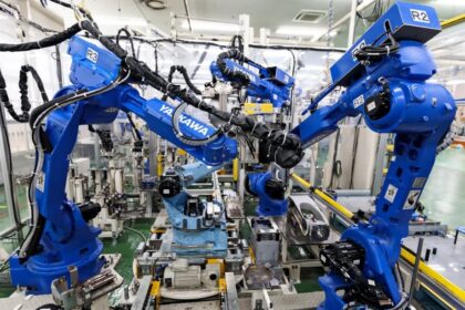
The scope is broad. Activity spans core manufacturing equipment, photoresist and specialty chemicals, packaging and testing hardware, and the electronic design automation software that designers need to translate blueprints into chips. A new manufacturing footprint is taking shape in Shenzhen, where three sites tied to Huawei and close partners are moving forward with city backed financing. While Huawei runs one complex, chip equipment maker SiCarrier and memory producer SwaySure operate the other two. Staff and know how move between the sites, allowing common process development and shared troubleshooting.
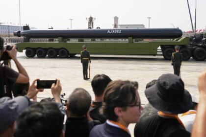
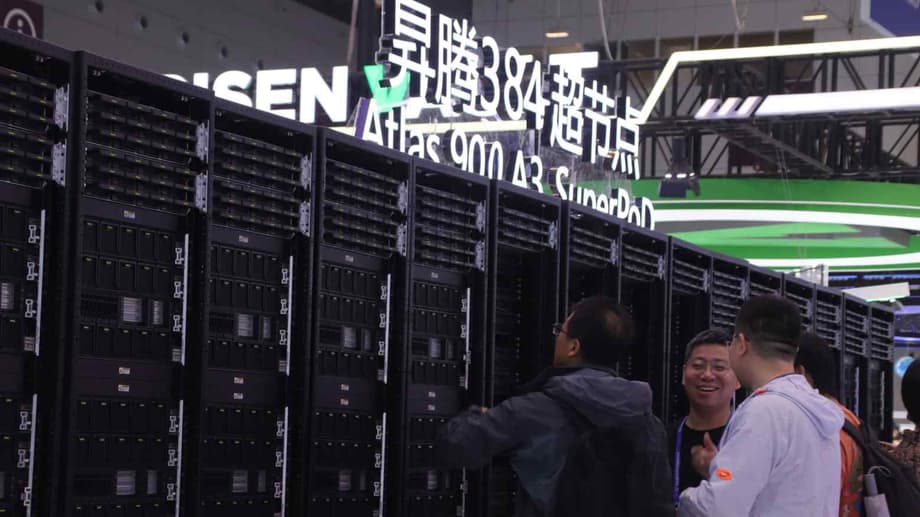
Behind the construction sits an investment program that gathered pace after the company came under United States export controls in 2019. Public tallies show Huawei and related funds have invested in more than 60 chip related businesses. Affiliates are now consolidating domestic rivals, expanding capacity, and launching alternatives to imported components. The goal is to secure supplies for flagship devices such as the Mate smartphone series and for data center products like the Ascend AI processors, while reducing exposure to foreign chokepoints.
Why Huawei is rebuilding the chip supply chain
Export controls limit what Chinese buyers can purchase in advanced logic, AI accelerators, chipmaking tools, and design software. The United States has tightened rules several times since 2019, adding categories such as high bandwidth memory and newer AI models. Key partners in Japan and the Netherlands aligned controls on lithography and other tools. This year, Taiwan also added Huawei and Semiconductor Manufacturing International Corporation to a list of entities that require approval for sensitive technology transactions. That step complicates chip design support and specialty materials that once flowed from the island to Chinese customers.
Constraints forced Huawei to replace core inputs and reroute development. Before restrictions, the company relied on Intel, Qualcomm, Broadcom, and TSMC. After controls took hold, it deepened ties to domestic suppliers such as SMIC for wafer fabrication and BOE Technology for displays. At the software layer, Huawei built out HarmonyOS as an alternative to Google mobile services that it can no longer pre install, and it pushed cloud and enterprise offerings to diversify revenue.
Beijing matched those moves with policy and funding. National programs including the Big Fund and the current five year plan channel resources into lithography, materials, advanced packaging, and design software. Leadership changes have centralized science and technology decision making. In that context, Huawei has shifted from a telecom champion to a supply chain coordinator, pulling equipment makers, materials firms, and chip designers into a common pipeline aimed at self reliance.
What the buildout looks like on the ground
In Shenzhen, three facilities linked to Huawei and its partners are designed to feed one another. Huawei runs a line aimed at smartphone processors and Ascend AI chips. SiCarrier provides wafer fabrication equipment and process engineering, while SwaySure focuses on memory. Local funding supports the complex, and shared teams move across sites as needed. The structure resembles an internal network of specialized suppliers that report into a central program office rather than a single vertically integrated plant.
The technology path leverages deep ultraviolet lithography (DUV), which is available domestically, rather than extreme ultraviolet lithography (EUV), which is restricted. DUV cannot draw the smallest features in one exposure, so engineers turn to multiple patterning, splitting the pattern into several aligned passes. Huawei has secured a patent covering self aligned quadruple patterning, a method that uses spacers and careful etch sequences to create very fine lines with DUV. This approach can reach feature sizes seen at nodes such as 7 nm, although it raises cost and makes yields and throughput harder to manage.
Design software is another critical piece. Electronic design automation, or EDA, is the toolchain that turns a chip architecture into a layout matched to a specific manufacturing process. Many leading tools originate in the United States and face license restrictions. Domestic vendors are moving to fill the gap for DUV based processes. Qiyunfang, a unit tied to SiCarrier, recently introduced two EDA products with independent intellectual property. Huawei is believed to validate and tune these flows for its needs, step by step replacing imported tools where controls apply.
Materials and testing are advancing in parallel. Photoresist, the light sensitive coating used in lithography, has been a chokepoint. Jiangsu HHCK Advanced Materials, in which Huawei holds a small stake, acquired a domestic competitor to scale volume and broaden coverage. In chemicals, Huawei is supporting the buildout of Zhuhai Cornerstone as a full line supplier that can compete with global incumbents. Downstream, Maxone Semiconductor has climbed into the global top tier of MEMS probe cards, the precision fixtures that connect a wafer to a tester. Huawei’s Hubble arm owns a meaningful stake. Maxone plans to use capital raised through the local market to localize inputs it still imports and to expand production for customers that include major chip designers, foundries, and outsourced assembly and test providers in China.
The investment map
Huawei’s investment arms have seeded a wide range of suppliers since 2019. Hubble has placed money into equipment, materials, and testing firms that fill gaps exposed by export controls. Vertilite, where Huawei holds a small stake, opened a new facility for compound semiconductors used in optics and power electronics that underpin telecom gear and data center networks. Shanghai Winscene and Aerotech are expanding production in optoelectronics and motion control that support high speed interconnects and semiconductor tool subsystems. The supply base is also moving in electronic materials and photoresist, where local firms are buying rivals to gain scale and process depth.
The pattern is consistent. Huawei spreads risk through minority stakes, shares engineers where needed, and then writes purchase orders that give a local champion the volumes required to mature. When a bottleneck emerges, associated firms turn to acquisitions or targeted R&D to close the gap. That method is now visible across materials, photoresist, EDA, and equipment. On the computing side, Huawei continues to develop Ascend AI accelerators and server CPUs, and it is investing in advanced packaging to boost performance where lithography is constrained. China is also embracing RISC V as an open instruction set, with large internet companies building toolchains and operating systems that avoid licensing barriers.
Constraints that still shape Huawei’s plan
EUV remains off limits, and that reality shapes everything. DUV based multiple patterning can deliver smaller features, but it drives up exposure counts and process steps, which in turn raise cost and hit yields. Many advanced inputs remain hard to replace at scale. High bandwidth memory, certain packaging films, advanced metrology, and leading edge deposition tools are still dominated by foreign vendors. Domestic alternatives are advancing, yet ramping to high volume on a schedule is difficult for complex tools and materials.
The AI stack is another challenge. High performance accelerators succeed only with a mature software ecosystem. Nvidia built CUDA over many years, creating a moat of compilers, libraries, and developer habits. Huawei and other Chinese firms are building compilers and frameworks tuned to their chips, aided by national computing projects that pool clusters across provinces. Progress is real, though developer migration takes time. Any new round of export controls can also force abrupt changes in specifications or suppliers, which is why Huawei keeps parts of its program quiet and works through partners to reduce attention on individual breakthroughs.
What it means for global supply chains
The semiconductor market is splitting into overlapping regional blocs. Huawei’s buildout gives China a more complete ecosystem that can support mature nodes and mid range logic with domestic tools and materials, and it is pushing the limits of DUV for advanced devices. Global companies face longer lead times, stricter compliance checks, and the need for localized bills of material to satisfy various national rules. Procurement leaders must track whether a module includes restricted content and whether a supplier sits on sanction lists across the United States, Taiwan, or Europe.
For U.S. chip makers, lost sales to China have weighed on revenue and jobs. That fallout has helped drive debates in Washington over tax credits and tighter coordination with allies to avoid one sided rules. A larger U.S. fab footprint can improve resilience, while growing Chinese capacity at 28 nm, 40 nm, and 55 nm creates new dependencies in non leading edge parts such as power management chips, image sensors, and microcontrollers. Huawei’s consolidation of local suppliers points to a more resilient Chinese stack, even as gaps persist at the cutting edge. The net effect is a semiconductor market with more regional redundancy, more compliance costs, and a slower pace for cross border technology sharing.
Key Points
- Huawei and affiliates are accelerating acquisitions and factory builds to create a self sustaining chip supply chain in China.
- More than 60 investments since 2019 target materials, equipment, EDA, packaging, and testing.
- A Shenzhen network of three sites run by Huawei, SiCarrier, and SwaySure shares staff and technology with city backed support.
- Huawei relies on DUV with multiple patterning, and has a patent covering self aligned quadruple patterning to push toward advanced nodes.
- Domestic EDA offerings are emerging, with Qiyunfang releasing tools tailored to local processes.
- Materials buildout includes photoresist and chemicals, with HHCK and Zhuhai Cornerstone scaling to replace imports.
- Maxone has moved into the global top tier of MEMS probe cards, with Hubble as a shareholder, to strengthen testing capacity.
- Taiwan now restricts business with Huawei and SMIC, aligning with allied export control policies.
- Huawei is developing Ascend AI chips and advancing HarmonyOS while expanding advanced packaging to improve system performance.
- Key constraints remain in EUV tools, high bandwidth memory, advanced materials, and software ecosystem maturity.