AI data moves to light as GlobalFoundries integrates Singapore AMF
GlobalFoundries has acquired Singapore headquartered Advanced Micro Foundry, a specialist in silicon photonics, in a move that pushes optical technology to the center of artificial intelligence infrastructure. The deal, with terms undisclosed, combines AMF’s 15 plus years of photonics manufacturing and intellectual property with GlobalFoundries’ global footprint. Company leaders say the combined operation becomes the largest silicon photonics pure play foundry by revenue, positioned to serve AI data centers, high speed communications, sensing, and emerging quantum systems. The acquisition is paired with a new research partnership in Singapore with the Agency for Science, Technology and Research, known as A*STAR, and plans for a silicon photonics center of excellence focused on next generation materials and links at 400 gigabits per second.
- AI data moves to light as GlobalFoundries integrates Singapore AMF
- Why silicon photonics matters for AI and advanced networks
- What the AMF deal adds to GlobalFoundries
- New R and D center in Singapore and a long term A*STAR partnership
- Voices from the companies
- How this shift fits the global race to optical connections
- Technology primer: from wafer size to co packaged optics
- Risks, integration, and what to watch
- Impact on Singapore and Asia’s chip ecosystem
- What to Know
Silicon photonics places light based components like waveguides and modulators alongside standard electronics on silicon. It replaces copper traces for many short and long distance data links with optical fibers and integrated optics. That shift reduces power draw and heat, and it delivers far higher bandwidth between servers, accelerator racks, and storage systems. With AI training clusters moving petabytes every hour inside data centers, and copper connections nearing their physical limits, optical pathways have become a priority for the sector.
Why silicon photonics matters for AI and advanced networks
Modern AI relies on vast networks of GPUs, custom accelerators, and high speed storage. Moving data between those components often dominates both power budgets and performance. Copper cables and electrical SerDes links lose signal strength at high frequencies and over distance, which forces repeaters and higher voltage swings. That increases energy use and latency. Optical links transmit data as light, which travels long distances with minimal loss and minimal cross talk, while using far less energy per bit.
Silicon photonics integrates optical functions on a silicon wafer alongside control electronics. Foundries fabricate waveguides that route light, modulators that encode data, and photodetectors that convert light back into electrical signals. Integrated approaches replace discrete transceiver modules with smaller, cooler, and often cheaper optical engines. The net effect is higher throughput per rack, lower cooling requirements, and improved reliability for hyperscale data centers and telecom networks.
The technology is also flexible. It supports pluggable transceivers that upgrade existing switches, and it supports co packaged optics that place optical engines adjacent to switch or accelerator silicon within a single package. Co packaged optics shortens the electrical path to only a few millimeters inside the package, then uses fiber for longer runs. That design improves energy use and signal integrity as link speeds climb from 400G to 800G and beyond.
What the AMF deal adds to GlobalFoundries
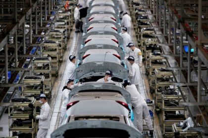
Advanced Micro Foundry is recognized as the first dedicated silicon photonics foundry. The company, spun out from Singapore’s Institute of Microelectronics at A*STAR in 2017, provides manufacturing, prototyping, and testing for customers across telecommunications, data centers, LiDAR, and sensors. AMF employs about 250 people and serves a global customer base from a 200 millimeter wafer platform, with a roadmap to 300 millimeter production as volumes grow.
By acquiring AMF, GlobalFoundries gains mature process design kits, device libraries, and a team with deep experience in photonic device integration and test. The company can respond to demand in long haul optical communications, inside the data center links, and specialty markets such as automotive sensing and quantum photonics. The combined scale also lets customers source from multiple geographies and qualify second sources, which reduces supply risk for critical infrastructure projects.
GlobalFoundries said its existing silicon photonics capabilities in the United States will be complemented by Singapore based manufacturing for worldwide customers. The aim is to accelerate time to market for optical transceivers, co packaged optics, and integrated photonic solutions that meet the rising bandwidth and efficiency needs of AI and cloud operators.
New R and D center in Singapore and a long term A*STAR partnership
GlobalFoundries plans to establish a silicon photonics center of excellence in Singapore that will work with A*STAR on materials and device research targeting 400 gigabits per second links and faster. That speed benchmark aligns with current data center cycles, where 400G and 800G are the standard building blocks for switch and server connectivity, and operators are already evaluating next step modules.
The company said the Singapore R and D effort will feed directly into its photonics platform and product roadmap. Singapore’s early investment in photonics and quantum research, plus its existing semiconductor talent base, make it a practical location to scale manufacturing while pushing device physics and process innovations. GlobalFoundries employs about 3,800 people in Singapore across multiple fabs, a base that eases transitions from lab results to production lines.
The move also shows how public research can translate into commercial capability. AMF’s origins within A*STAR’s Institute of Microelectronics illustrate a pipeline from academic research to industrial scale solutions. The new collaboration aims to shorten that path for future photonic platforms, including novel materials that support higher speed, lower loss, and lower power optical links.
Voices from the companies
GlobalFoundries chief executive Tim Breen framed silicon photonics as a core requirement for current and future AI infrastructure. He said the company will use AMF’s capacity and expertise to expand its product roadmap for optical solutions that cut power and increase throughput inside data centers and across wide area networks.
Silicon photonics technology is essential for AI infrastructure. As data moves faster and workloads grow more complex, the ability to move information with greater speed, precision and power efficiency is now fundamental to AI data centers and advanced telecom networks.
AMF chief executive Jagadish CV highlighted the fit between the two companies and the potential to reach more markets with a broader portfolio.
AMF and GF share a vision of innovation and close customer partnerships to deliver differentiated solutions. With complementary technology portfolios, we look forward to advancing silicon photonics for a broader range of markets and customers.
How this shift fits the global race to optical connections
Optical links have become a strategic focus across the industry. Network chipmakers and hyperscale operators are pushing toward pluggable and co packaged optics to keep up with AI scale clusters. Companies such as Nvidia have worked with leading foundries to package networking silicon with optical connections. Venture backed players including Ayar Labs, Celestial AI, and Lightmatter are building optical chip to chip connections, and some use GlobalFoundries for manufacturing. In quantum computing, GlobalFoundries works with PsiQuantum on photonic based chips for large scale quantum systems.
More capacity in Singapore, alongside existing operations in the United States and Europe, gives GlobalFoundries a diversified manufacturing base. That helps cloud providers and telecom carriers that want multi region sourcing for critical components. It also positions Singapore as a hub for design, fabrication, and test of silicon photonics as adoption widens across data communications, sensing, and computing.
The acquisition also extends a long running connection between GlobalFoundries and Singapore. In 2010 the company acquired Chartered Semiconductor, which expanded its presence in the country. The AMF transaction adds a specialization in photonics that aligns with the current wave of AI infrastructure spending.
Technology primer: from wafer size to co packaged optics
Two details help explain why this deal could change the pace of photonics adoption: wafer size and packaging.
From 200 millimeter to 300 millimeter wafers
AMF’s current production uses 200 millimeter wafers. GlobalFoundries plans to scale to 300 millimeter as customer demand increases. Larger wafers mean more die per wafer, improved economies of scale, and often more advanced toolsets. Moving a photonics platform to 300 millimeter can reduce cost per function and support higher volumes of transceivers and optical engines. The transition requires careful process transfer and qualification to preserve optical performance, such as low propagation loss in waveguides and consistent modulator behavior across wafers.
From pluggable modules to co packaged optics
For decades, network equipment has relied on pluggable optical modules that slot into the front of switches. Those modules will remain important, since they let operators upgrade optics without replacing entire systems. Co packaged optics introduces a change. Optical engines sit on the same substrate as a switch ASIC or accelerator, with very short electrical traces. That minimizes signal loss, lowers power, and supports higher aggregate bandwidth per chassis. Foundry level integration of photonics and electronics is a key enabler for this architecture, and it is a focus area for GlobalFoundries’ roadmap.
Why 400G matters
Modern racks in AI data centers move data in multiples of 100G lanes. A 400G transceiver typically uses four 100G lanes, while 800G doubles that. Achieving reliable 400G and 800G at scale with low power consumption is a practical stepping stone toward terabit class links. Research into materials, modulators, and low loss waveguides at those speeds helps the industry lower cost per bit and power per bit, the two metrics that dominate data center network design.
Risks, integration, and what to watch
Scaling a silicon photonics platform is not trivial. Yield depends on optical loss, device uniformity, packaging alignment, and test coverage. Moving from 200 millimeter to 300 millimeter requires process control across more die and often across new tools. Integration of teams and PDKs must be careful to keep design rules stable for customers. Supply chains for lasers, materials, and advanced packaging must also scale to match wafer output.
Customer adoption cycles are another variable. Many cloud operators upgrade optics on multi year timelines tied to switch silicon and fabric architecture refreshes. Convincing customers to migrate from pluggable modules to co packaged optics will depend on proven reliability, service models, and the ability to repair or replace optics in the field.
Competition is intense. Leading foundries and network silicon vendors are all investing in optical interconnects. The companies that can combine high yield manufacturing, robust design ecosystems, and strong packaging partnerships will win the most sockets in next generation switches and AI clusters.
Impact on Singapore and Asia’s chip ecosystem
Singapore has invested for years in photonics, quantum research, and semiconductor manufacturing. The country’s semiconductor sector contributes a significant share of gross domestic product, and public agencies have launched programs to strengthen design, advanced packaging, and specialty materials. AMF’s journey from a research institute spinoff to a global supplier, and now part of a leading contract chipmaker, illustrates how publicly funded science can seed exportable expertise.
The new center of excellence and expanded production could attract startups and multinationals that want to design and manufacture optical engines in Asia while maintaining access to North American and European foundry capacity. Singapore’s role as a neutral, stable hub is appealing for supply chain resilience. For deep tech startups working on photonics, quantum, and sensing, easier access to prototyping, pilot runs, and volume ramps within the same ecosystem can shrink time to market.
For GlobalFoundries, the communications infrastructure and data center segment is already one of the fastest growing lines of business. Executives have signaled that silicon photonics could reach a multibillion dollar run rate before the end of the decade if adoption continues on today’s trajectory. The AMF acquisition and the A*STAR partnership are designed to keep that trajectory on track by increasing capacity, speeding innovation, and reducing regional bottlenecks.
What to Know
- GlobalFoundries acquired Singapore based Advanced Micro Foundry to expand silicon photonics capacity and capability, with financial terms undisclosed.
- The combined operation positions GlobalFoundries as the largest silicon photonics pure play foundry by revenue.
- A new silicon photonics center of excellence in Singapore will partner with A*STAR on 400G and faster optical technologies.
- AMF adds a 200 millimeter platform, mature process design kits, and a global customer base, with plans to scale to 300 millimeter.
- Silicon photonics moves data with light, cutting power use and latency compared with copper, which is critical for AI data centers and telecom networks.
- GlobalFoundries aims to accelerate products from pluggable transceivers to co packaged optics for data communications and computing.
- Startups such as Ayar Labs, Celestial AI, Lightmatter, and quantum player PsiQuantum are part of the broader shift to optical connections.
- Key execution challenges include yield, process transfer to larger wafers, advanced packaging, and customer adoption cycles.