
A tiny semiconductor channel gives superconducting current a preferred direction
Researchers at the University of Tokyo and New York University have built a semiconductor device that carries current without electrical resistance more easily in one direction than the other. The device reached a maximum superconducting diode efficiency of 20%, combining electrical control with magnetic effects in a channel just 100 nanometres long.
Contents
- A tiny semiconductor channel gives superconducting current a preferred direction
- What the researchers actually built
- How neighbouring layers share their properties
- Why clean boundaries mattered
- Voltage sets the limit for current without resistance
- What the 20% diode efficiency means
- The magnetic history changes the response
- Where the current flows is still being investigated
- What changes for future superconducting circuits
- Key Points
The findings, published in Communications Materials on November 5, 2026, come from experiments at 0.03 kelvin, close to absolute zero. A device without a gate electrode carried a superconducting current of up to 3.00 microamperes. In devices fitted with a gate, applying a negative voltage reduced the maximum current that could flow without resistance.
The University of Tokyo team included doctoral researcher Hirotaka Hara, Associate Professor Le Duc Anh and Professor Masaaki Tanaka, working with NYU researchers including doctoral researcher Lukas Baker and Professor Javad Shabani. Their structure combines aluminium, indium arsenide and gallium antimonide containing iron, bringing superconductivity and magnetism into the same semiconductor current path.
The immediate result is a laboratory building block for controlling superconducting current. The University of Tokyo's November 5 announcement identifies possible applications in electronics that consume less energy and future quantum circuits. The work is currently at the stage of investigating operating principles and improving control.
What the researchers actually built
The device is a lateral Josephson junction with a semiconductor channel. A Josephson junction connects two superconducting electrodes through a short intervening material. Quantum effects allow current to cross that material without an accompanying voltage, even when the material would not become superconducting on its own.
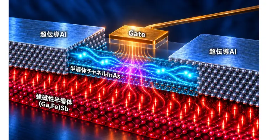
Here, two aluminium electrodes sit on a semiconductor structure, with an exposed indium arsenide channel between them. The channel is approximately 100 nanometres long and 5 micrometres wide. Its width is therefore about 50 times its length.
Indium arsenide provides the main path for electrical current. Beneath it lies gallium antimonide containing iron, written as (Ga,Fe)Sb, which supplies magnetic influence. The aluminium electrodes supply superconducting influence. A gate electrode above the channel lets the researchers change its electrical properties with voltage.
The transistor description reflects that gate control. More precisely, the Communications Materials paper describes lateral Josephson junctions made from an Al/InAs/(Ga,Fe)Sb structure. The device brings the voltage control familiar from semiconductor transistors into a superconducting junction.
How neighbouring layers share their properties
Aluminium becomes superconducting when sufficiently cold. In that state, electrons form pairs that can carry current without electrical resistance. Magnetism, by contrast, involves the alignment of the tiny magnetic properties of electrons, known as spins. Ordinary superconductivity and ferromagnetism tend to work against each other, making their combination difficult.
The researchers used proximity effects to bring both influences into indium arsenide. A proximity effect occurs when contact with one material changes the behaviour of electrons in a neighbouring material. Aluminium induces superconducting behaviour in the channel, while the magnetic semiconductor beneath it can influence the same electrons.
The magnetic layer contained 14.6% iron and had an estimated Curie temperature of about 25 kelvin. The Curie temperature is the point above which a material loses its ferromagnetic ordering. At the much colder temperatures used for the superconducting measurements, the (Ga,Fe)Sb layer becomes electrically insulating, so current travels mainly through the indium arsenide.
This arrangement gives the layers different jobs: the indium arsenide conducts, the aluminium supports superconducting transport, and the semiconductor containing iron provides magnetic influence. Their shared boundaries are central to making those jobs work together.
Why clean boundaries mattered
The team grew the structure using molecular beam epitaxy, a method that deposits carefully controlled layers in a vacuum. All the layers were made without exposure to air, reducing contamination at the boundaries where the materials meet.
The semiconductor stack included a layer of indium arsenide 15 nanometres thick above a magnetic layer 20 nanometres thick. A thin cap of indium gallium arsenide, 5 nanometres thick, helped form the interface with the aluminium. The aluminium film was 26 nanometres thick.
The semiconductor layers were grown at 250 degrees Celsius to limit the separation of iron within the magnetic material. The aluminium was subsequently deposited at a temperature below minus 40 degrees Celsius. This sequence allowed the team to prepare the different materials under conditions suited to each.
Electron microscopy showed a clean, atomically sharp boundary between the aluminium and the semiconductor cap. The paper also records local disorder or defects in that cap. Electrical measurements nevertheless showed that the interface allowed superconducting transport to pass effectively into the semiconductor.
Voltage sets the limit for current without resistance
The experiments measured how much current the junction could carry before electrical resistance appeared. That upper limit is called the critical current. Below it, a superconducting junction can carry current without generating heat through electrical resistance; above it, a voltage develops.
At 30 millikelvin, equivalent to 0.03 kelvin, a junction without a gate reached a critical current of 3.00 microamperes. The researchers then tested junctions with a gate electrode. Making the gate voltage more negative removed electrons from the indium arsenide channel and lowered its critical current.
The gate therefore adjusted how much superconducting current the channel could support. The paper also reports that the critical current levelled off under positive gate voltages, while leakage current through the gate remained below roughly 10 picoamperes across the measured voltage range.
The team found further evidence of coupling between the aluminium and semiconductor through multiple Andreev reflections. These are repeated conversions between electron and hole excitations at a superconducting boundary. Their signatures appeared in the electrical measurements up to the sixth order, helping the researchers assess how readily superconducting transport crossed the interfaces.
Those measurements gave a superconducting energy gap of 171 microelectronvolts. The gap is an energy scale associated with the paired electrons that sustain superconductivity. Together, the reflection measurements and gate response show how the semiconductor carries current under the influence of its superconducting neighbours.
What the 20% diode efficiency means
The diode effect appeared when the researchers applied a magnetic field perpendicular to the junction. The critical current then depended on the direction in which current flowed. One direction could support a larger current without resistance than the reverse direction.
For a current between those two limits, the junction remained superconducting in one direction and developed resistance in the other. At currents below both limits, either direction could still support superconducting transport. The directional effect therefore operates within a particular range of current.
The researchers calculated diode efficiency by subtracting the smaller critical current magnitude from the larger one, then dividing by their sum. The maximum value was 20%, reached near a minimum in the junction's magnetic interference pattern.
That definition makes the result easier to picture. An efficiency of 20% corresponds to a larger critical current 1.5 times the smaller one. For illustration, limits of 1.5 and 1.0 in the same current units would give a difference of 0.5 divided by a sum of 2.5, or 20%. Those illustrative numbers explain the ratio; the measured maximum is the reported 20%.
The efficiency figure describes the asymmetry between current directions. The maximum occurred near a minimum of the interference pattern, where superconducting transport was reduced by the applied magnetic field. The largest directional contrast and the largest current capacity therefore occurred under different operating conditions.
The magnetic history changes the response
The junction also responded differently depending on whether the external magnetic field was being increased or decreased. The field at which superconducting current reached its maximum shifted with the direction of the field sweep. Researchers observed this behaviour repeatedly in several devices, including junctions with and without gates.
This dependence on past conditions is called hysteresis. Magnetic materials often show it because their internal magnetic alignment retains some memory of an earlier applied field. In these junctions, the repeated shifts are consistent with a magnetic contribution to superconducting transport from the neighbouring (Ga,Fe)Sb layer.
The current varied with magnetic field in a series of peaks and minima known as a Fraunhofer interference pattern. Such patterns arise because superconducting current behaves as a quantum wave: contributions from different parts of a junction can reinforce or weaken one another as the magnetic field changes.
The measured patterns contained uneven peaks, abrupt magnetic flux jumps and differences between opposite current directions. Near one maximum, the oscillation period was 0.14 millitesla, compared with a geometrical estimate of 1.13 millitesla. The paper derives an effective magnetic flux focusing factor of 8.2 from that difference.
The authors identify several possible contributors to that concentration of magnetic flux, including the response of the aluminium electrodes, magnetic fields from the underlying layer, and uneven magnetic or current distributions. The overall pattern supports studying the device as a coupled magnetic and superconducting system.
Where the current flows is still being investigated
The researchers also examined whether current was spread evenly across the channel. They applied a mathematical analysis to a region of the interference pattern without abrupt flux jumps and found a tendency for superconducting current to concentrate near the physical edges.
Microscope images showed no visible shortening of the junction near those edges. The authors discuss transport along the channel edges as one possible contributor to the unusual magnetic response and directional behaviour.
The precise balance of mechanisms remains unresolved. The paper discusses magnetic influence from the lower layer, interactions linking electron motion and spin, and possible transport near the edges. Magnetic domains, trapped flux and variations introduced during fabrication may also affect parts of the interference pattern.
For future device design, understanding that balance matters in concrete terms. Engineers would need to know which material properties and geometrical features reliably set the preferred current direction, the usable current range and the response to gate voltage.
What changes for future superconducting circuits
Josephson junctions are central components in superconducting quantum circuits. Replacing a simple barrier with a semiconductor allows electrical adjustment of the junction, while placing a magnetic semiconductor nearby adds another way to influence its behaviour.
The Tokyo and NYU work combines those features in one structure: gate control changes the critical current, and magnetic effects alter the current response and its directional preference. That combination offers a material platform for investigating circuit elements with more adjustable behaviour.
The University of Tokyo identifies electronics with lower energy consumption and quantum computers more resistant to errors as longer term goals. The demonstrated measurements concern individual junctions operating at extreme cold. Cooling remains a practical requirement alongside the benefit of current flowing without resistance.
The researchers plan to improve the magnetic layer and investigate more closely how voltage and magnetism act on superconducting current. Their next scientific task is to turn the observed effects into more predictable control, supporting the design and fabrication of more varied quantum circuits. No timetable was given for a practical computing device.
Key Points
- The University of Tokyo and NYU developed lateral Josephson junctions combining aluminium, indium arsenide and a magnetic semiconductor containing iron.
- The channel measured about 100 nanometres long and 5 micrometres wide, with experiments conducted at 0.03 kelvin.
- A junction without a gate carried up to 3.00 microamperes without resistance; negative gate voltage reduced the critical current in gated devices.
- Under a perpendicular magnetic field, the maximum superconducting diode efficiency reached 20% near an interference minimum.
- Repeated hysteresis across several devices was consistent with magnetic influence on superconducting transport.
- The findings were published on November 5, 2026. Further work will examine the mechanisms and improve control for possible future quantum circuits.