
Tainan prepares for another generation of chipmaking
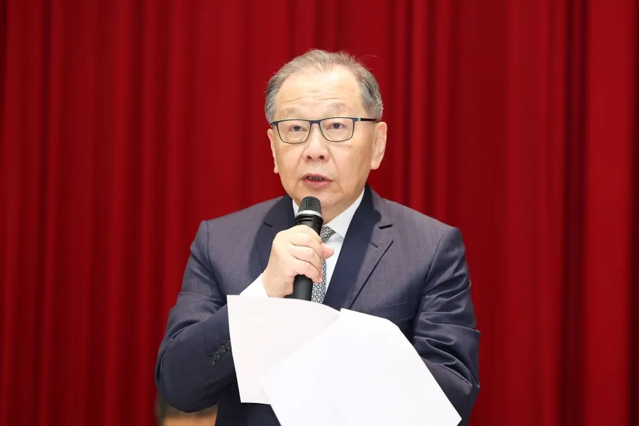
Taiwan plans to begin development procedures in 2027 for a large new science park in Tainan intended to accommodate future factories using 1 nanometer chip technology, National Science and Technology Council Minister Wu Cheng-wen said on November 2, 2026. The proposal puts land and infrastructure planning at the center of preparations for Taiwan's next generation of semiconductor manufacturing.
Contents
- Tainan prepares for another generation of chipmaking
- Shalun emerges as a possible location
- What 1 nanometer means for a factory
- Tainan already has expansion dates to meet
- Four pillars connect chips with other industries
- AI infrastructure is part of the 2027 budget direction
- Why moving data with light matters
- Robotics could create work for traditional suppliers
- Research partnerships underpin the expansion
- Key Points
Speaking at the 2026 IEEE Asian Solid-State Circuits Conference, Wu said the new park would join a network of 18 parks managed by three science park administrations under the council. Adding one would bring that network to 19, extending a system that connects manufacturing companies with research institutions, suppliers and skilled workers.
Taiwan Semiconductor Manufacturing Co., or TSMC, is the potential manufacturer at the center of the proposal. The government wants to prepare space for more advanced production as the company's 2 nanometer technology enters mass production. Wu also outlined a broader economic goal: use semiconductor earnings, research capabilities and artificial intelligence infrastructure to help industries beyond chipmaking.
Shalun emerges as a possible location
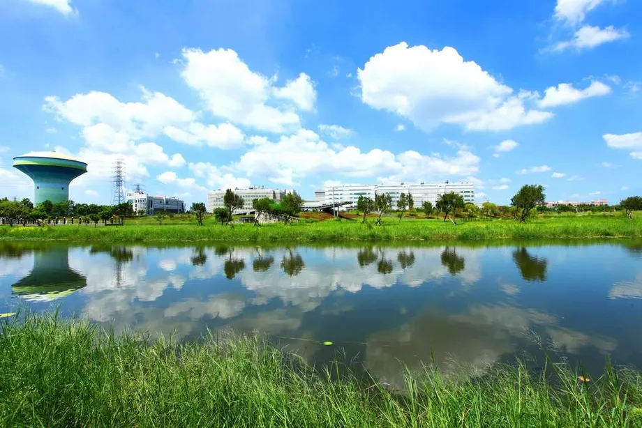
People familiar with the planning identified the Shalun area near Tainan's high speed railway station as a possible location. They described a potential complex of six large factories processing wafers measuring 12 inches across, with manufacturing using 1 nanometer or more advanced 0.7 nanometer technology. Their account also envisaged advanced packaging, the work of connecting chips and other components into a functioning product.
Those people said the Southern Taiwan Science Park administration was pursuing an expansion through the park's designated planning area. Such an approach would connect the proposed facilities with a wider development framework rather than treating them as an isolated factory project.
TSMC said Taiwan remained its principal base, that it was keeping its options open and that specific factory plans should follow its formal announcements. The exact site, investment amount, construction and production schedules, and proposed six factory configuration await company confirmation. Wu's announced milestone is the start of government development procedures in 2027.
What 1 nanometer means for a factory
A semiconductor factory, commonly called a fab, makes chips on thin discs known as wafers. Many chips are formed on each wafer before they are separated and prepared for use in devices. The proposed 12 inch facilities would use the large wafer format associated with advanced chip manufacturing.
The labels 2 nanometer, 1 nanometer and 0.7 nanometer identify generations of manufacturing technology. They help distinguish production processes rather than provide a single literal measurement of every feature inside a chip. Moving to a newer generation involves changes in how extremely small electronic components are made and connected.
Wu said future production would require progress in manufacturing technology alongside land, electricity, water and a complete supply chain. His announcement connects those two tasks: engineers develop the process, while public authorities prepare the physical conditions for factories to operate. Starting park procedures in 2027 gives the government a planning milestone while technical development continues.
Tainan already has expansion dates to meet
The proposed park would add another layer to Tainan's existing semiconductor expansion. TSMC Chairman and Chief Executive C. C. Wei announced an additional Tainan 3nm factory on October 15, with commercial production planned for the first half of 2028. Another Tainan project was already expected to begin mass production in the first half of 2027.
Tainan's government had pledged to help secure water, electricity and public facilities for that expansion while speeding up administrative procedures. According to the city government, TSMC had completed 20 fabrication, packaging and testing facilities at the Southern Taiwan Science Park, invested more than NT$1.86 trillion there and created more than 11,300 jobs.
The announced milestones now span several years:
- October 15, 2026: Wei announces another Tainan factory using 3 nanometer technology.
- November 2, 2026: Wu outlines a large new Tainan science park intended for future 1 nanometer fabs.
- 2027: Development procedures for the proposed park are expected to begin; an existing Tainan 3 nanometer project is scheduled to enter mass production in the first half.
- First half of 2028: Commercial production is planned at the additional 3 nanometer factory.
Four pillars connect chips with other industries
Wu described Taiwan's chip strategy through four pillars: maintaining its advantages, deepening international cooperation, driving innovation through AI, and building sustainability and adaptability. The proposed park belongs to the first effort, while much of his speech addressed how semiconductor strength could support a wider range of businesses.
He identified four areas of focus: high performance computing, quantum computers, intelligent robots and silicon photonics. High performance computing uses powerful systems to carry out demanding calculations. Silicon photonics brings optical technology together with semiconductor manufacturing to move information using light.
Wu also named space technology, unmanned vehicles, next generation communications and biomedical care as fields that could benefit from Taiwan's semiconductor and AI capabilities. His argument was that chips provide a technological foundation for these activities, while investment and access to computing resources can help more companies put that foundation to use.
AI infrastructure is part of the 2027 budget direction
Wu said government planning would direct more tax revenue generated by high technology industries toward helping other sectors change how they operate. The 2027 budget would reflect that direction, particularly through an expansion of AI computing infrastructure.
Computing infrastructure means the processors, servers and supporting systems needed to run AI software. Access matters because developing and using sophisticated AI tools requires more than an ordinary office computer. Wu said traditional industries and emerging fields should also be able to obtain those resources.
The proposal responds to concerns that semiconductor companies attract too much of Taiwan's talent and technology funding. Wu's response was to connect the sector's success with investment elsewhere: keep supporting advanced manufacturing while using part of the resulting public revenue to broaden access to technology. For companies outside the chip industry, the practical policy issue is access to computing capacity that can support their own work.
Why moving data with light matters
AI data centers need to move large amounts of information as well as perform calculations. Wu used silicon photonics to explain why Taiwan's technology plans extend beyond the processors themselves. Faster computation needs communication systems that can carry data quickly while using less energy.
He said optical communication should develop beyond connections inside individual equipment racks toward networks that use light more widely. The proposed direction involves replacing some copper connections with optical fiber to increase bandwidth and improve energy efficiency. Bandwidth describes how much information a connection can carry within a given time.
Wu linked that communications development with the foundations needed for emerging industries, including robotics. His examples show why the policy covers several connected technologies: processors handle calculations, communication links move information, and the wider system allows machines and services to use the results.
Robotics could create work for traditional suppliers
Metal, plastics, chemical and materials businesses were central to Wu's explanation of how technology investment might reach beyond established semiconductor companies. He said robotics could create a large supplier network and give traditional manufacturers opportunities to move into applications with greater commercial value.
Wu used metal products as an example. Materials used in ordinary hardware could instead become important robot components. In his assessment, moving into those applications could improve company profits and create room for higher employee pay.
The example gives the government's diversification proposal a concrete industrial route. Existing manufacturers would contribute materials and components to new products, rather than all being expected to become chipmakers or software companies. Wu presented the prospect of better margins and wages as an intended benefit of that shift.
Research partnerships underpin the expansion
Wu traced Taiwan's semiconductor development over roughly 50 years to cooperation among government, industry and universities. He pointed to Hsinchu Science Park's proximity to the Industrial Technology Research Institute, National Chiao Tung University and National Tsing Hua University as an example of how research, training and manufacturing grew together.
The council funds academic research and establishes national research centers with costly equipment, materials and specialist staff that university researchers can share. Wu connected these platforms with the training of more advanced integrated circuit designers, the people who plan how a chip's electronic components work together.
Wu said Taiwanese companies produced more than 90% of the world's AI servers and ranked first in wafer manufacturing. He used that industrial position to support a call for wider international collaboration, including efforts to bring quantum computing and high performance computing together. Quantum computers use different physical principles from conventional computers, making their integration a research and engineering task rather than simply an increase in server numbers.
International companies were being invited to cooperate, Wu said. Taken together, his proposals connect a local land development plan in Tainan with research partnerships abroad and a domestic budget intended to spread access to AI resources across more industries.
Key Points
- Taiwan expects to begin development procedures in 2027 for a large Tainan science park intended to accommodate future 1 nanometer factories.
- Wu Cheng-wen announced the plan on November 2 at the 2026 IEEE Asian Solid-State Circuits Conference.
- People familiar with planning identified Shalun as a possible site and described six factories for 1 nanometer or 0.7 nanometer production.
- TSMC said specific factory plans would be subject to its formal announcements.
- The proposed park would join a network of 18 parks managed by three science park administrations.
- The 2027 budget is intended to support broader industrial transformation, including expanded access to AI computing resources.
- Wu identified high performance computing, quantum computers, intelligent robots and silicon photonics as areas of focus.