
Taiwan expansion targets a critical AI supply bottleneck
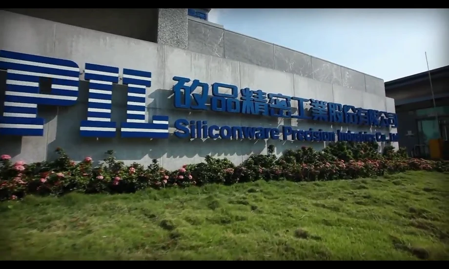
Siliconware Precision Industries (SPIL), the semiconductor packaging and testing company owned by ASE Technology Holding, announced on November 18, 2026, a multibillion dollar agreement with Nvidia aimed at tripling its advanced packaging capacity in Taiwan by the middle of 2029.
Contents
- Taiwan expansion targets a critical AI supply bottleneck
- What the agreement commits the companies to build
- Why packaging matters as much as making chips
- Four production steps under one arrangement
- Substrate expansion brings another Taiwan factory into focus
- Nearly $3 billion also supports Amkor expansion
- New platforms need factories and system builders to move together
- Testing and optical capacity have their own targets
- The milestones from 2026 to 2029
- Key Points
Nvidia's supply chain announcement, dated November 17, describes multibillion dollar funding for SPIL and an increase in contracted advanced packaging capacity dedicated to Nvidia by mid-2029. SPIL supplied the more specific target of reaching three times current capacity.
The agreement addresses a manufacturing constraint that SPIL says has already delayed AI system deliveries across the industry. Making more silicon chips is one part of supplying more AI computers. Manufacturers also need enough capacity to connect, package and test those chips before they can enter finished systems.
SPIL plans new production lines, factory upgrades and greater automation. Nvidia says the lines will cover bumping, interposer wafer fabrication, assembly and testing, giving it a connected production service across several essential steps.
The Taiwan project sits within a wider expansion involving suppliers in the United States, South Korea and other manufacturing locations. Nvidia is arranging additional capacity for substrates, chip packaging, testing and complete systems as it prepares production for current and future computing platforms.
What the agreement commits the companies to build
SPIL's target would add capacity equal to twice its present level, bringing the total to three times the starting point. The companies have not disclosed the exact funding amount, payment terms, starting production volume or allocation among individual Taiwan factories.
Nvidia describes its commitment as funding under an agreement spanning several years. For SPIL, that provides a basis for planning production lines and factory improvements around Nvidia's future requirements. For Nvidia, the arrangement secures contracted access to manufacturing services that are in heavy demand.
SPIL chairman and chief executive C.W. Tsai described the agreement as a deepening of the companies' relationship:
SPIL is proud to strengthen our collaboration with NVIDIA.
Tsai said the project would strengthen SPIL's ability to support future packaging technologies and deliver the performance and reliability required by coming AI systems. The expansion therefore combines more production capacity with work on the manufacturing processes those systems will need.
Why packaging matters as much as making chips
Advanced packaging connects semiconductor components so they can operate together in a compact, high performance product. A chip leaving a wafer factory still needs electrical connections, physical protection and testing before it can become part of a reliable computing system.
AI hardware puts demanding requirements on those connections. Processors must move large amounts of information quickly while controlling electricity use. Packaging helps determine how closely components can be placed together and how efficiently information travels between them.
SPIL says demand for advanced packaging is far above existing supply. Its expansion is designed to support products with strict requirements for computing performance, bandwidth, power efficiency and system integration. Bandwidth means the amount of information a connection can carry in a given time.
Nvidia executive vice president of operations Debora Shoquist explained the company's reason for expanding manufacturing commitments:
Our supply chain is a strategic advantage.
Shoquist said the partner agreements extend Nvidia's manufacturing foundation across components, advanced packaging and system production. The practical aim is to deliver complete computing platforms, which depend on all these stages being ready together.
Four production steps under one arrangement
SPIL's new lines will provide what the industry calls turnkey support: a coordinated service covering several production stages rather than requiring a customer to arrange each stage independently. Nvidia's announcement identifies four parts of the project:
- Bumping creates tiny electrical connection points on semiconductor wafers.
- Interposer wafer fabrication makes an intermediate layer that helps connect components inside an advanced package.
- Assembly brings the components together into the package.
- Testing checks whether the finished product operates as required.
SPIL also plans to upgrade factory facilities and increase automation. It says these changes are intended to shorten production lead times and make manufacturing more resilient. Coordinating the stages matters because a delay at any one can hold up the finished product, even when the other stages have spare capacity.
Substrate expansion brings another Taiwan factory into focus
Kinsus Interconnect Technology is planning a related expansion at its Youth campus in Taoyuan, Taiwan. Under a new Nvidia agreement, it intends to increase advanced ABF package substrate capacity dedicated to Nvidia to more than 3.5 times current levels.
A package substrate is a finely wired base that supports a chip package and connects it to the wider electronic system. ABF refers to the insulating material used in these advanced substrates. The substrate must accommodate many small connections while meeting demanding electrical and manufacturing requirements.
Kinsus expects production to begin in the second half of 2027, with the additional capacity targeted for the third quarter of 2028. Its relationship with Nvidia already spans more than a decade, according to Kinsus chief executive and president Scott Chen.
The Kinsus and SPIL targets measure different production activities. Kinsus is expanding substrates to more than 3.5 times its current Nvidia allocation; SPIL is targeting three times current advanced packaging capacity. Together, the projects show why supplying more AI systems requires expansion across several linked factory processes.
Samsung Electro-Mechanics has also amended its existing substrate agreement with Nvidia to improve capabilities at current factories. That arrangement builds on manufacturing operations in Sejong and Busan, South Korea, supporting Nvidia's computing and high speed networking technologies.
Nearly $3 billion also supports Amkor expansion
Nvidia's advanced packaging commitments extend beyond Taiwan. Agreements announced with Amkor Technology in July and October 2026 total nearly $3 billion and support expansion in Arizona and South Korea.
Those Amkor agreements include prepayments to help the company increase manufacturing capacity for Nvidia's production needs over several years. Nvidia describes the SPIL commitment separately as multibillion dollar funding, with its detailed financial structure undisclosed.
Amkor president and chief executive Kevin Engel said the investments would serve several generations of AI platforms. Planning across multiple generations gives a supplier time to develop packaging technology and install capacity before a customer's production requirements grow.
The geographic pattern is concrete: SPIL is expanding advanced packaging in Taiwan, Amkor is adding capacity in the United States and South Korea, and substrate suppliers are expanding or improving operations in Taiwan and South Korea. Nvidia is securing several manufacturing routes while increasing the amount of work individual partners can handle.
New platforms need factories and system builders to move together
Nvidia says Vera Rubin NVL72 and Vera CPUs began volume shipments in the third quarter of 2026, using TSMC's 5 nanometer and 3 nanometer manufacturing technologies and CoWoS advanced packaging. Volume shipment means products are being delivered at a commercial production scale.
TSMC supplies chip manufacturing and packaging technology within that network. Its senior vice president and deputy co-chief operating officer, Kevin Zhang, said the relationship allows the companies to plan future technology requirements and prepare manufacturing capabilities as Nvidia introduces platforms.
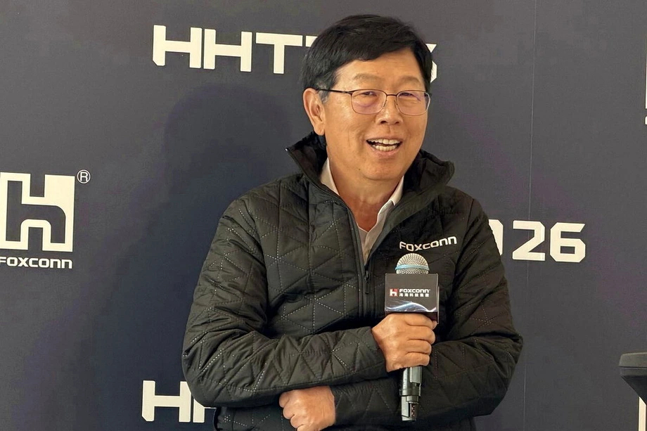
Foxconn is deepening its work with Nvidia on future graphics processor and networking platforms. Chairman Young Liu pointed to Foxconn's production network across Asia, North America and Europe as the foundation for supporting larger production volumes.
The manufacturing push connects with Nvidia's DSX POD deployment plan, announced in October, which uses factory assembly and testing to prepare containerized AI infrastructure before shipment. That design targets deployment in as little as 14 days once a destination has the necessary power, cooling, networking and other infrastructure ready.
SPIL's packaging lines address an earlier part of that delivery chain. Packaged and tested processors must reach system builders before racks can be assembled, checked and shipped. Faster installation at a data center depends on having those components ready upstream.
Testing and optical capacity have their own targets
Nvidia's November announcement builds on October commitments involving Amkor, IBIDEN, King Yuan Electronics (KYEC), Samsung Electro-Mechanics, SPIL and Unimicron. Those plans included an aggregate increase in substrate capacity to 2.5 times its starting level over three years, alongside a doubling of semiconductor testing capacity from 2026 to 2027.
Testing is another essential production gate. As factories produce more chips and packages, testing operations must grow with them so completed hardware can be checked before delivery. KYEC president Gauss Chang said the company's expansion into the United States would place testing capabilities closer to Nvidia's growing American manufacturing supply chain.
SPIL also has a distinct optical engine expansion plan. Nvidia says the October commitments called for optical engine capacity to reach 15 times its starting level by mid-2027, with another doubling targeted by the end of 2028. Optical engines convert electrical signals into light for data transmission.
Each target tracks a different manufacturing activity and schedule: advanced packaging at SPIL, optical engines at SPIL, substrates across suppliers and semiconductor testing. Together, they describe a broader effort to increase the flow of usable components through the AI hardware supply chain.
The milestones from 2026 to 2029
The announced schedules stretch across several years, with substrate production, testing and optical equipment reaching milestones before SPIL's full advanced packaging target. The main dates are:
- July and October 2026: Nvidia announced Amkor agreements totaling nearly $3 billion.
- Third quarter of 2026: Nvidia says Vera Rubin NVL72 and Vera CPUs began volume shipments.
- November 17 and 18, 2026: Nvidia and SPIL announced the expanded Taiwan packaging arrangement.
- Mid-2027: SPIL targets optical engine capacity at 15 times its starting level.
- Second half of 2027: Kinsus expects production to begin under its new substrate arrangement.
- Third quarter of 2028: Kinsus targets its additional substrate capacity.
- End of 2028: SPIL aims to double optical engine capacity again from the mid-2027 target.
- Mid-2029: SPIL targets advanced packaging capacity at three times its current level.
Nvidia's release describes the expansion schedules as projections subject to manufacturing, technology, demand and other risks. For customers waiting for AI equipment, the practical benefit will arrive as each production stage becomes operational and supports larger deliveries. Taiwan's role grows across that chain, from substrates and chip manufacturing to packaging, testing and system assembly.
Key Points
- SPIL says its multibillion dollar Nvidia agreement targets three times current Taiwan advanced packaging capacity by mid-2029.
- Nvidia confirms funding and increased contracted capacity dedicated to its products.
- New SPIL lines will cover bumping, interposer wafer fabrication, assembly and testing.
- Kinsus plans Nvidia substrate capacity above 3.5 times current levels, with added capacity targeted for the third quarter of 2028.
- Amkor agreements totaling nearly $3 billion support packaging expansion in Arizona and South Korea.
- Testing and optical engine projects have separate capacity targets and deadlines.