
Huawei puts its three dimensional chip strategy into phones
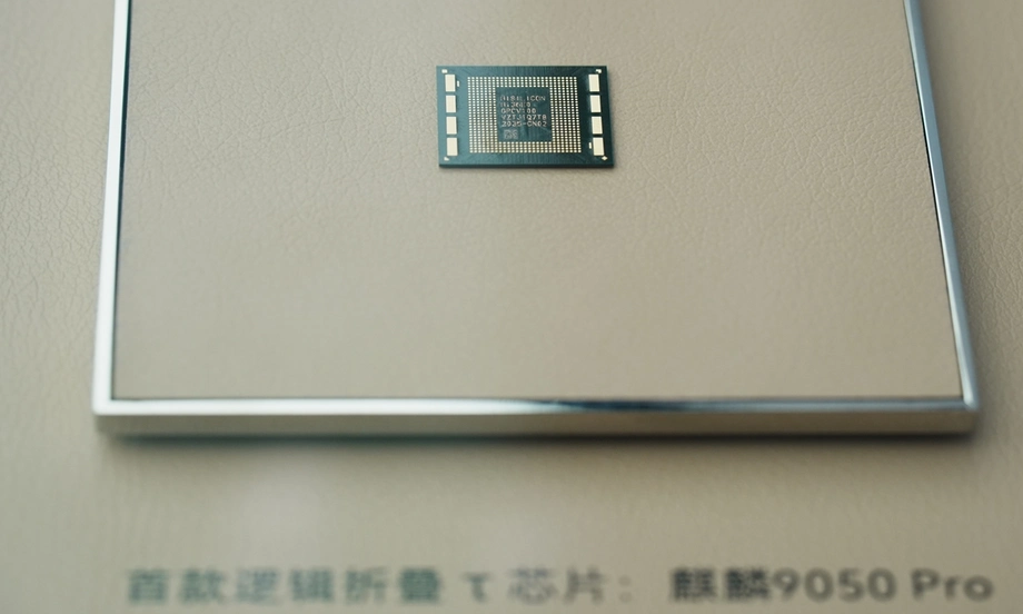
Huawei says its Kirin 9050 series has brought LogicFolding into mass production, increasing transistor density by 53.5% by arranging computing circuits across connected layers. At an October 13, 2026, briefing at its Lianqiuhu research center in Shanghai, the company described a way to improve chips by shortening the journeys that electrical signals make inside them.
Contents
- Huawei puts its three dimensional chip strategy into phones
- How LogicFolding shortens the journey
- What the performance numbers mean
- Millions of bonds connect the layers
- AI models get a smaller memory footprint
- From a May announcement to October disclosures
- A route around equipment limits, with costs attached
- What Huawei is targeting for 2027 and 2031
- Why the ambition extends beyond smartphones
- Key Points
Huawei reported a 23% increase in CPU performance when multiple cores work together, a 40% increase in graphics rendering performance, and a 140% increase in artificial intelligence computing power compared with the previous generation. The higher specification Kirin 9050 Pro reportedly reaches 238 million transistors per square millimeter.
Xu Songyu, head of wireless terminal chip product management in Huawei's semiconductor business, said the series contains more than 50 million hybrid bonding points and more than 5 million effective signal interconnections. Those connections allow circuits on different layers to communicate through short vertical routes instead of relying on longer paths across a flat surface.
The development matters because restrictions have blocked Huawei's access to some of the world's most advanced chipmaking equipment. Huawei is pursuing improvements through circuit layout, connections and coordinated design while continuing to face limits in manufacturing technology.
The company identified the Mate 90 Pro Max as its test device and the Mate 80 Pro Max as the comparison device. Huawei's figures describe its own measurements; buyers still need independent testing to understand battery life, sustained gaming performance and AI responsiveness across everyday applications.
How LogicFolding shortens the journey
A transistor is a tiny electronic switch. Billions of these switches form the circuits that run software, draw graphics and process data. Their speed depends partly on how quickly signals can move between them.
Traditional scaling packs more transistors into a given area by making features smaller. LogicFolding instead distributes circuits across active silicon layers and joins them with dense vertical connections. A connection that previously crossed a large horizontal distance can take a shorter route between layers.
Huawei says the design expands the layout from one active layer to two. Its reported measurements show a 20% reduction in core routing lengths and reductions of up to 70% in key timing paths. These critical paths are routes whose delays can limit how quickly a circuit completes its work.
Xu described the chips as several bare silicon pieces, or dies, designed together as one complete processor. The placement of circuits and their connections is planned in three dimensions from the beginning, so the layers can share work efficiently.
Shorter wires can reduce resistance and unwanted electrical loading, allowing signals to arrive sooner and with less energy. Stacking also concentrates activity into a smaller footprint, making the removal of heat a central engineering task.
What the performance numbers mean
Huawei's reported gains cover three different parts of the processor. The CPU handles general computing tasks, the GPU draws graphics, and the NPU is designed for AI calculations. A 23% increase in CPU performance means a result 1.23 times the previous level; a 140% increase in NPU computing power means 2.4 times the previous level.
The company also reports substantial power savings. At comparable performance, its measurements put NPU power consumption 66% lower, GPU consumption 58% lower and CPU core consumption 41% lower. Huawei's October briefing separately described a 41% improvement in the energy efficiency of the Kirin 9050 Pro's large CPU cores.
Energy efficiency measures the work completed for a given amount of energy, while power consumption measures how quickly energy is used. The two measures require their own test conditions. Huawei also said it had reduced operating voltages and clock speeds to help control heat.
The reported Kirin 9050 Pro specifications include a CPU with nine cores, a primary core operating at 3.1 GHz, a Maleoon 920 GPU and a Da Vinci NPU. For a phone owner, the practical value will depend on how those components perform together during a long game, a demanding application or repeated AI requests.
Millions of bonds connect the layers
Hybrid bonding joins silicon surfaces through extremely small electrical contacts. Huawei says the Kirin 9050 Pro uses a bonding pitch of 1.5 micrometers, meaning the spacing between neighboring connection points is about 1.5 thousandths of a millimeter.
The connection figures need careful wording. Huawei's detailed breakdown gives more than 50 million bonding points and more than 5 million effective signal connections; another description from the October briefing calls more than 50 million connections high speed interconnect channels. The reported package breakdown puts the share carrying active signals at roughly 10% to 15%, so readers should distinguish the total physical connections from those used for signals.
Manufacturing those connections requires extremely accurate alignment, wafer thinning and surface smoothing. Small gaps or misaligned copper contacts can damage connections. Yield, the share of manufactured chips that work properly, becomes especially important when several active layers must function together.
Huawei has not disclosed the Kirin 9050 Pro's foundry, manufacturing node, production yield or full benchmarking conditions. Those details would help assess the cost of making the chips and the repeatability of the reported gains.
AI models get a smaller memory footprint
Huawei says the Kirin 9050 series can run an AI model with 30 billion parameters using an additional 2.5 GB of memory. Parameters are numerical values learned during training that help a model produce its answers.
The model uses a Mixture of Experts design, often shortened to MoE. This divides work among specialized parts of a model and activates selected parts for a task. That can reduce the computing needed for each response compared with activating the entire model.
Huawei reports a 25% improvement in model loading performance and a 75% reduction in memory use compared with the previous generation. On that comparison, the new memory requirement is one quarter of the earlier level. The company describes the 2.5 GB figure as additional memory use, rather than the phone's total memory requirement.
Running an AI model on a phone allows supported tasks to be processed locally, without sending every request to a remote server. For users, loading time and memory use matter alongside computing power: a model must fit alongside the operating system and other applications, then respond quickly enough to be useful.
From a May announcement to October disclosures
Huawei introduced the broader principle behind LogicFolding on May 25 at the 2026 IEEE International Symposium on Circuits and Systems. He Tingbo, president of Huawei's semiconductor business, presented what the company calls the Tau Scaling Law.
The company's Tau Scaling Law announcement proposed time scaling as a guiding principle for semiconductor development. The Greek letter tau represents a time constant, a measure connected to how quickly an electrical circuit responds. Huawei's approach seeks to reduce delays from individual devices through to complete computing systems.
The rollout has moved through several stages:
- May 25, 2026: Huawei presented the Tau Scaling Law and said Kirin chips arriving in autumn would be the first to use LogicFolding.
- September 12, 2026: Sales of the Mate XT 2 Ultimate Design, reported to contain the Kirin 9050 Pro, began in China.
- October 1, 2026: Huawei launched the Mate 90 Pro Max Collector's Edition with the Kirin 9050 Pro.
- October 13, 2026: Huawei detailed the architecture in Shanghai and said its 2027 Kirin chips were already undergoing testing.
Huawei says it designed and mass produced 381 chips under the broader Tau framework over six years. Xu said exploration of LogicFolding itself began four years ago. The framework covers several kinds of optimization, while LogicFolding is the specific circuit architecture now entering Kirin products.
A route around equipment limits, with costs attached
Huawei's work takes place under restrictions that block access to advanced extreme ultraviolet lithography machines made by the Dutch company ASML. These machines help manufacturers create very small circuit features. TSMC has begun volume production of chips using its 2 nanometer process, while Huawei is seeking gains through a different combination of manufacturing and design choices.
Neil Shah, vice president of research at Counterpoint Research, identified heat, packaging and production yield as major tests for Huawei's approach.
"However, this parallel semiconductor path is still unproven at scale. This approach can introduce tough thermal constraints and packaging complexities that can hit the manufacturing yields," Shah said.
Huawei's financial figures show the scale of its investment. Research and development spending reached 121.38 billion yuan in the first half of 2026, up 25.2% from a year earlier and equivalent to 25.9% of revenue. Net profit fell 36% to 23.81 billion yuan during the same period.
The consumer rollout begins at the expensive end of the market. The Mate XT 2, a phone whose screen folds into three sections, went on sale in China at prices ranging from 19,999 to 24,999 yuan. Huawei also says shipments of devices using Kirin chips have exceeded 100 million since their return in August 2023, giving future processor generations a substantial product base.
What Huawei is targeting for 2027 and 2031
Huawei plans to reduce hybrid bonding pitch from 1.5 micrometers to 1 micrometer in 2027. With the same layout, reducing spacing in both directions would theoretically allow about 2.25 times as many connection positions per unit area. Actual usable density depends on routing, power delivery and manufacturing requirements.
The company says Kirin 2027 test silicon already has more than 100 million vertical interconnections, and Xu said test results were meeting expectations. Huawei has also described a target of 720 nanometers for bonding pitch within three years and possible future designs with three or four active layers.
For 2031, Huawei's official target is transistor density equivalent to a 14 angstrom, or 1.4 nanometer, process. Density describes how many transistors fit into an area. A manufacturing process also determines transistor behavior, power characteristics and production requirements, so Huawei's stated target concerns one part of chip performance.
Paul Triolo, head of technology for Asia and the Americas at DGA Group, has pointed to continuing challenges in manufacturing yield, power, heat and device performance. Xu likewise listed design tools, compensation for manufacturing variation, energy control, interconnections between layers and benchmarking methods among the tasks still ahead.
Why the ambition extends beyond smartphones
Huawei's Tau framework also covers software, processor architecture and large computing systems. At chip level, the company describes designing software and silicon together so instructions and data move efficiently. At system level, its UnifiedBus approach aims to reduce communication delays across large groups of computing equipment called SuperPoDs.
Mateo Valero, director of the Barcelona Supercomputing Center, said success depends on coordinating applications, software, processor architecture, memory and transistors.
"The transistor is important, but what matters now is how an entire system behaves," Valero said.
That presents a larger test than a smartphone launch. A data center must keep many processors supplied with data while managing communication, electricity use and cooling. Huawei has described plans to extend LogicFolding to enterprise computing and to launch an Ascend 990 AI chip by 2030.
Huawei's progress in domestic AI computing also affects Nvidia's commercial opportunities in China. George Chen, partner and co-chair of digital practice at The Asia Group, said the window for Nvidia to sell advanced chips such as the H200 into China was narrowing as local alternatives developed.
For now, Huawei's concrete achievement is the reported commercial deployment of a processor designed around tightly connected active layers. The next milestones are the 2027 Kirin generation, denser bonding and evidence of how the architecture performs over sustained workloads and larger production volumes.
Key Points
- Huawei says Kirin 9050 chips bring LogicFolding into mass production, increasing transistor density by 53.5%.
- Reported gains include 23% higher CPU performance, 40% higher graphics performance and 140% higher NPU computing power.
- The design uses two active layers, with bonding points spaced 1.5 micrometers apart.
- Huawei says its 2027 Kirin chips are in testing and plans to reduce bonding pitch to 1 micrometer.
- The company's 2031 target is transistor density equivalent to a 1.4 nanometer process.
- Heat, manufacturing yield, design tools and production costs remain central engineering challenges.