
A 0.7 nanometer step toward smaller electronic switches
South Korean researchers have created the main components of a transistor inside a single thin film by replacing selected atoms, achieving current control close to the theoretical limit for conventional transistors at room temperature. The technique works in layers about 0.7 nanometers thick and could simplify the construction of extremely small electronic devices.
Contents
- A 0.7 nanometer step toward smaller electronic switches
- Why assembling these materials is difficult
- Three replacement atoms, three different jobs
- How the team chose the layer and location
- A lower barrier where current enters
- Switching close to the room temperature limit
- Insulation that gives the gate close control
- A stacked circuit operated at 1 volt
- Publication and the move toward larger wafers
- Key Points
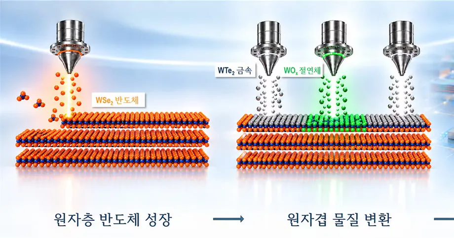
The team, led by Cho Moon-ho, director of the Institute for Basic Science Center for Van der Waals Quantum Solids and a distinguished professor at Pohang University of Science and Technology, started with tungsten diselenide. By replacing its selenium atoms with oxygen, sulfur or tellurium, the researchers made regions that insulate, carry current or help current enter the semiconductor.
The resulting transistor needed a gate voltage change of 61.3 millivolts to increase current tenfold, compared with a theoretical minimum of about 60 millivolts at room temperature. Its current when switched on was more than 10 million times its current when switched off.
The researchers also built a small circuit from vertically stacked transistors that reversed an electrical signal at 1 volt. Together, the results connect precise control of individual material layers with a working circuit, while leaving the expansion to semiconductor manufacturing as the next major task.
Why assembling these materials is difficult
A transistor is an electrically controlled switch. It needs a semiconductor channel through which current travels, an insulating layer that allows a gate to control that channel, and electrodes that connect the device to the rest of a circuit. Each part has a different job, so making their boundaries work well is essential.
Semiconductors described as two dimensional remain useful even when only a few atomic layers thick. Their surfaces, however, do not readily form chemical bonds with other materials. This makes it difficult to coat them evenly with an insulating film. Attaching metal electrodes directly can also damage the contact surface or create electrical resistance that restricts current.
Moving separately prepared films into place and stacking them offers another route, but adds manufacturing steps. The Korean team instead created several of the required materials within the starting film, reducing the need to bring different films together.
Three replacement atoms, three different jobs
Tungsten diselenide, written as WSe2, has a layer of tungsten atoms between selenium atoms above and below. The researchers kept the tungsten while selectively replacing the selenium. Changing the surrounding atoms changed how each treated region behaved electrically.
Oxygen produced tungsten oxide, an insulator. Sulfur produced tungsten disulfide, an n-type semiconductor. Tellurium produced tungsten ditelluride, a conductive semimetal used at the connection between the metal electrode and semiconductor.
- Unconverted tungsten diselenide provided the p-type semiconductor region.
- Tungsten oxide provided electrical insulation for gate control.
- Tungsten disulfide supplied an n-type semiconductor for complementary devices.
- Tungsten ditelluride helped charge move between an electrode and the semiconductor.
The terms p-type and n-type describe how electrical charge travels through a semiconductor. In an n-type material, electrons carry the current. In a p-type material, current is described through the movement of holes, the positively charged vacancies left where electrons are missing. Both types are needed for the complementary circuit the team demonstrated.
How the team chose the layer and location
Temperature and reaction gas pressure allowed the researchers to control how deeply the chemical changes travelled into the film. They used the tiny gaps between material layers as barriers that limited the movement of reacting atoms, helping stop a conversion from spreading into the next layer.
Each controlled step corresponded to an atomic layer about 0.7 nanometers thick. A nanometer is one billionth of a meter. This figure describes the thickness of the material layer being converted; the fabrication method also required control over where the conversion happened across the surface.
Semiconductor processing masks supplied that second kind of control. Like a precisely patterned covering, a mask exposes selected areas while protecting others. Combining masks with control of reaction depth let the researchers form different materials at chosen locations and layers within one film.
A lower barrier where current enters
The tungsten ditelluride contact region addressed a different problem from switching the transistor: getting charge into the semiconductor efficiently. Even a channel that responds well to its gate can perform poorly if its electrical connections make charge transfer difficult.
The researchers measured an energy barrier of 35.5 millielectronvolts at the electrode to semiconductor connection. They described this as about one third of the barrier with a directly attached metal electrode. An energy barrier is the obstacle charge carriers must overcome when crossing between materials.
Expressed as a comparison, a barrier reduced to one third is roughly 67 percent lower. The measured improvement concerns charge transfer at the contact. Power consumption across a complete circuit also depends on its operating voltage, leakage current and switching activity.
Switching close to the room temperature limit
The transistor's 61.3 millivolt measurement describes how sharply it switches as the gate voltage changes. Engineers call this the subthreshold swing: the change in gate voltage needed to change the current by a factor of ten while the device moves toward its conducting state.
A smaller value means a smaller voltage adjustment produces a large current change. Compared with the approximate room temperature limit of 60 millivolts for conventional transistor operation, the measured value was just 1.3 millivolts higher, or about 2.2 percent above that benchmark.
The ratio between the current in the on and off states exceeded 10 million to one. This measures how strongly the device separates its conducting and nonconducting states. Low current in the off state matters because electricity leaking through idle transistors wastes energy.
The contact barrier, switching response and current ratio describe three related parts of the device's performance. The contact helps charge enter, the gate regulates its passage, and the difference between on and off current shows how effectively the transistor acts as a switch.
Insulation that gives the gate close control
The tungsten oxide region supplied the insulating layer. This layer must separate the gate electrically from the channel while allowing the gate's electric field to control current. Producing it by converting part of the starting material tackles the difficulty of depositing a uniform coating on a two dimensional semiconductor.
The team described its insulation as meeting the International Roadmap for Devices and Systems target of an equivalent oxide thickness of 1 nanometer or less. Equivalent oxide thickness, usually shortened to EOT, expresses an insulator's electrical performance as the thickness of a reference silicon dioxide layer with the same capacitance.
EOT therefore describes electrical behaviour rather than simply the physical thickness of the material. The researchers were quoted giving an EOT below 1 nanometer; published numerical descriptions also included 0.3 to 0.4 nanometers and approximately 1 nanometer. The exact value is unresolved in those descriptions, while all place the insulation at or within the stated roadmap target.
A stacked circuit operated at 1 volt
The researchers went beyond testing a single transistor by stacking a p-type transistor and an n-type transistor vertically to make a complementary inverter. An inverter is a basic digital circuit: a high input produces a low output, and a low input produces a high output.
The circuit reversed signals at an operating voltage of 1 volt. Building it required the different semiconductor types to work together, connecting the material conversion method to a basic function used in digital electronics.
Vertical construction also connects the experiment to the team's plans for three dimensional integrated circuits. Arranging devices above one another offers a route to putting more circuitry within the same surface area, provided the materials and processing can be controlled throughout the stack.
Cho, the IBS center director and POSTECH distinguished professor, described the connection between the material technique and device fabrication:
This study integrates a basic materials science technique of atomic-scale material manipulation with modern semiconductor technology,
Publication and the move toward larger wafers
The research paper is titled Modular van der Waals MOSFETs through layer-by-layer chalcogen substitutions. MOSFET is the name of a widely used family of transistors controlled by an insulated gate. Chalcogens are the chemical family that includes oxygen, sulfur, selenium and tellurium, the elements central to the substitutions.
The announcement and publication dates were described as follows:
- October 15, 2026: The Ministry of Science and ICT was described as announcing the modular transistor research.
- October 16, 2026, at 3 a.m. Korean Standard Time: The ministry placed the Science publication at this time. Other descriptions dated the public announcement to October 16.
The next stage is to apply the method to other two dimensional semiconductors and expand it across wafers, the broad substrates used to manufacture many semiconductor devices together. Achieving uniform and reproducible atom replacement across those surfaces is a requirement for industrial use. No timetable for manufacturing deployment was given.
The practical change sought by the team is specific: create useful materials in place rather than repeatedly transfer and join separate films. At a larger scale, that could reduce assembly complexity while preserving the close gate control and improved contacts measured in the experimental devices.
Kim Seong-su, director of the Ministry of Science and ICT's R&D Policy Office, said the government would continue supporting basic and foundational research so that original technologies could contribute to South Korea's industrial competitiveness. The researchers' next work will focus on larger processing areas, additional materials and stacked integrated circuits.
Key Points
- The Korean team formed key transistor components by selectively replacing selenium atoms in tungsten diselenide.
- Temperature, gas pressure and masks controlled conversion in layers about 0.7 nanometers thick and at selected surface locations.
- The contact energy barrier fell to 35.5 millielectronvolts, about one third of the value with direct metal contact.
- A gate voltage change of 61.3 millivolts increased current tenfold, close to the approximate 60 millivolt room temperature limit.
- The current ratio between the on and off states exceeded 10 million to one.
- A vertically stacked complementary inverter reversed signals at 1 volt.
- Uniform processing across semiconductor wafers is the next requirement for industrial application.