
A semiconductor mission built around power savings
South Korea is targeting a rise in AI computing efficiency from about two tokens per watt today to 200 by 2035, bringing Samsung Electronics, SK hynix and semiconductor equipment maker Jusung Engineering into a government research mission. The plan combines an 8.8 times improvement in computing performance with an 11.4 times reduction in power use, aiming for roughly 100 times more computing output per watt.
Contents
- A semiconductor mission built around power savings
- What the 100 times target actually means
- Why memory is at the center
- A memory stack combining DRAM and NAND
- Three stages lead toward 2035
- Packaging becomes part of the computing plan
- Who will guide the research
- Public funding and the decisions still ahead
- Key Points
The Ministry of Science and ICT launched operating and technical committees for the K Moonshot semiconductor mission in Seoul on October 14. More than 20 experts from government, industry, universities and research institutions are participating. Their task is to develop foundational technologies that address two connected limits on AI computing: the energy consumed by moving data and the difficulty of supplying processors with that data fast enough.
The semiconductor effort is one of 12 missions in K Moonshot, a program that combines AI with science and technology to tackle national challenges. Its central ambition is to build computing systems around memory, rather than treating memory as a separate store that must constantly send information to a processor.
The ministry has allocated 25 billion won for key projects in the year following the launch. That is an initial allocation, not a stated budget for the entire program through 2035. The distinction matters because the proposed work extends from devices and manufacturing processes to memory stacks, packaging and complete computing platforms.
What the 100 times target actually means
The mission measures its ambition through tokens per watt. Tokens are the units of text processed by many generative AI models, sometimes whole words and sometimes parts of words. Here, the measure is intended to express how much AI processing a system can deliver for the power it consumes.
The arithmetic behind the target is consistent: 8.8 multiplied by 11.4 equals 100.32. Raising performance while reducing the power needed to deliver it would therefore produce approximately the stated improvement. Moving from two to 200 tokens per watt also represents a factor of 100.
These are research targets, not results from a completed chip. The announcement does not establish which AI model, workload or computing configuration will be used to measure success. It also does not specify whether the power measurement will cover individual chips or a wider system. Those choices will matter when comparing future demonstrations with the starting point.
A gain in efficiency does not automatically mean a corresponding fall in total electricity consumption. If substantially more AI work is performed, total consumption can still increase. The mission's measurable promise is more computation for each watt, with separate goals for performance and power use.
Why memory is at the center
The ministry identifies memory bottlenecks and rising power consumption as core constraints. In conventional computing, processors repeatedly retrieve data from memory and send results back. When processors can work faster than data can reach them, part of their capacity goes unused. Moving that data also consumes energy.
Computing centered on memory seeks to reduce that burden by placing computation within memory or closer to it. The aim is broader than making a memory chip faster: it involves changing how processing, storage and data movement work together.
This approach connects the mission's two numerical goals. Reducing delays in data movement can help processors complete more work, while shortening or avoiding transfers can reduce energy use. Whether the planned technologies deliver both benefits at the required scale will need to be established through demonstrations.
The ministry's focus also reflects the expansion of AI beyond generative models running in large computing facilities. AI operating directly on devices must work within battery and heat limits. Physical AI, including robotics, must combine timely computation with power management. The announcement does not set separate performance targets for these applications, but identifies their growth as a reason to pursue more efficient chips.
A memory stack combining DRAM and NAND
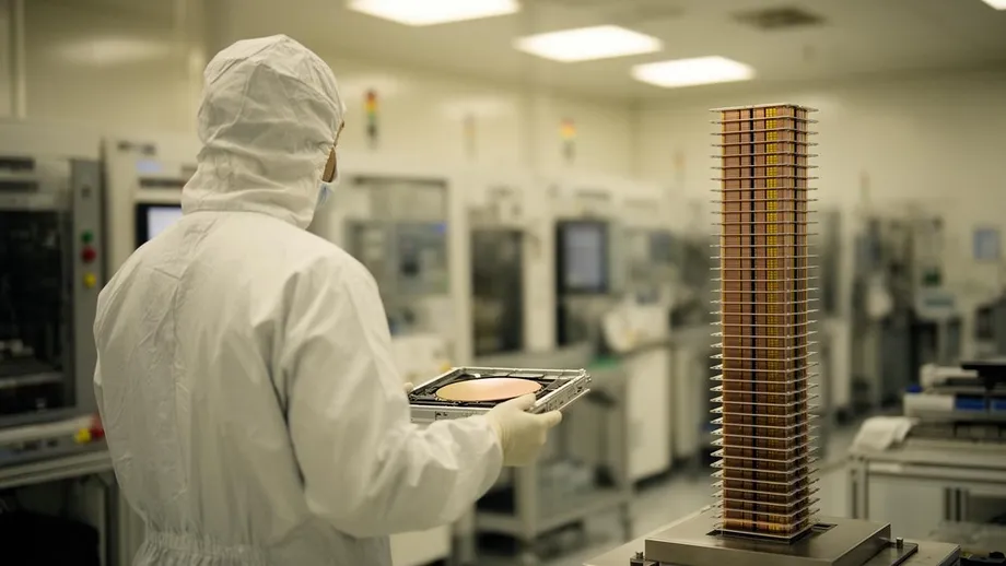
One of the mission's key projects is a proposed new form of high bandwidth memory, or HBM. It would vertically combine HBD, a memory component based on DRAM, with HBF, a component based on NAND flash. The objective is to bring the speed of DRAM together with the larger storage capacity associated with NAND.
DRAM provides rapid access to working data, while NAND flash stores data without requiring continuous power. They serve different purposes and have different operating characteristics. Combining them is therefore more involved than simply adding extra layers to an existing memory stack.
The proposed design responds to the need to keep larger quantities of AI data accessible without allowing transfers between storage, memory and processors to dominate performance and energy use. Vertical stacking is intended to bring these functions together in a more compact arrangement.
The announcement does not give capacity, bandwidth, production yield or commercial release targets for this memory project. It should therefore be understood as a development direction, rather than a product announcement. Its value will depend on how successfully the different memory technologies operate together and how the resulting stack performs in a complete system.
Three stages lead toward 2035
The roadmap divides development into three stages, moving from very small semiconductor devices to stacked chips and then integrated platforms. It sets out the following sequence:
- October 14: The ministry launches the operating and technical committees in Seoul.
- 2026 to 2029: Development focuses on extremely fine semiconductor devices and processes.
- 2030 to 2032: The program advances stacked semiconductor technologies.
- 2033 to 2035: Work focuses on integrated platforms and demonstrations at the system level.
- 2035: The mission targets 200 tokens per watt, compared with about two at the stated starting point.
Reporting differs in its dating of the launch. One account explicitly gives October 14, 2026, while other accounts identify October 14 without specifying a year. The launch date and the roadmap should therefore be kept distinct rather than using an uncertain year to assign a calendar date to the funding described as being for next year.
The first stage includes device and process technology for circuits below one nanometer. A nanometer is one billionth of a meter. The announcement sets a direction for research at an exceptionally small scale, but does not explain exactly which feature dimensions the target refers to or provide a manufacturing schedule.
The final stage is especially important to the mission's stated purpose. A promising device or memory component will not by itself demonstrate 100 times greater computing efficiency. The technologies must be integrated and tested together to establish what they deliver as a working platform.
Packaging becomes part of the computing plan
The ministry also plans advanced packaging that brings together glass substrates, optical communications and computing chips. Packaging is the structure that connects and supports chips, allowing them to exchange data and operate as a system. In this mission, it is part of the technology being developed, not simply the last step after chip production.
Optical communications use light to carry information. Their inclusion places connections between components alongside devices and memory as areas for research. Glass substrates are also part of the planned integration work, although the announcement does not provide specifications or measured advantages for the proposed designs.
The broader strategy reflects a shift described by the ministry: competition is moving beyond shrinking a single chip toward integrating devices, manufacturing processes, memory, packaging and systems. Improving one component may deliver limited benefits if another component still restricts data movement or consumes too much power.
That is why the mission includes integrated demonstrations reflecting industrial demand. The aim is to test whether advances work together under useful computing conditions, rather than judging each research result only by its performance in isolation.
Who will guide the research
Kim Ji-young, the semiconductor program director, chairs the operating committee. Participants include the Ministry of Science and ICT, the National Research Foundation of Korea, Samsung Electronics, SK hynix and Jusung Engineering, alongside academic and research experts.
The operating committee will establish and revise research project plans, review major implementation matters and coordinate decisions. A separate technical committee will develop the technology roadmap, plan detailed projects, monitor research progress and manage targets. This divides responsibility between program direction and technical delivery.
At the launch meeting, participants discussed priorities for core technologies, goals for each stage, connections with existing semiconductor research programs and demonstrations shaped by industry demand. Jusung Engineering is expected to contribute to device and process development, bringing an equipment company's perspective into a group that also includes major memory manufacturers.
Kim Sung-soo, the ministry official responsible for research and development policy, said the mission should connect foundational research with industrial competitiveness:
We will concentrate the capabilities of industry, academia, and research institutions to proactively secure foundational technologies for future semiconductors and ensure that research outcomes translate into industrial competitiveness through the K-Moonshot semiconductor mission.
The committee launch establishes a governance structure. It does not, by itself, establish that the proposed technologies are ready for production or that participating companies have committed to particular commercial products.
Public funding and the decisions still ahead
The ministry expects public investment to support expensive technologies with substantial technical risk, including research that companies may struggle to finance alone. Universities, companies and research institutes will develop foundational technologies, while government and industry will jointly validate them through research projects.
The 25 billion won allocation gives the mission an initial funding commitment. The announcement does not provide a total budget through 2035, a division of funding among participants or an amount of matching corporate investment. Those omissions limit what can be concluded about the scale of the full effort.
Several technical details also remain unresolved publicly: the benchmark for measuring tokens per watt, the exact scope of the power measurement, specifications for the combined DRAM and NAND stack, and criteria for accepting integrated demonstrations. These are practical decisions that will determine whether progress can be measured consistently against the headline target.
The roadmap supplies broad development periods but no specific dates for further hearings, funding decisions or product releases. The next substantive work falls to the committees: turning the mission into detailed projects, assigning measurable goals and connecting the research with existing programs. The central test is whether advances across memory, devices and packaging produce the promised efficiency when combined.
Key Points
- South Korea aims to raise AI computing efficiency from about two to 200 tokens per watt by 2035.
- The target combines an 8.8 times performance improvement with an 11.4 times reduction in power use.
- Samsung Electronics, SK hynix and Jusung Engineering are participating alongside government, universities and research institutions.
- A proposed memory stack would combine DRAM based HBD with NAND based HBF.
- The roadmap covers fine semiconductor technologies in 2026 to 2029, stacked chips in 2030 to 2032 and integrated platforms in 2033 to 2035.
- The ministry has allocated 25 billion won for initial key projects, but has not stated a total budget through 2035.
- Benchmark details and commercial release dates have not been specified.