
A Texas chip project aims for Samsung's memory scale
Terafab, the semiconductor venture pursued by Tesla and SpaceX, has told equipment suppliers it wants capacity for about 1 million wafers a month, including 700,000 for memory chips and 300,000 for logic chips. The memory target alone approaches Samsung Electronics' current DRAM capacity of roughly 650,000 to 700,000 wafers a month.
Contents
- A Texas chip project aims for Samsung's memory scale
- What the million wafer target means
- Japanese suppliers face a compressed timetable
- Machines are only the first production test
- Intel technology and a dispute over control
- Why Musk wants development measured in weeks
- The dates that will measure progress
- A terawatt of chips is a separate ambition
- Who will fund the expansion?
- Key Points
The proposed expansion centers on Grimes County, Texas, where Governor Greg Abbott's office put the first phase of the Gibbons Creek project at more than $16.8 billion on August 6, 2026. Elon Musk has since accepted that spending across the venture could eventually reach $1 trillion, with investment spread over successive phases.
Terafab has yet to produce chips. Its nearer milestones are a first SRAM test chip around May or June 2027 and volume production in the third quarter of 2028. Supplier discussions have placed the million wafer target in 2032, although another description of those discussions puts that scale after 2032.
The project would supply chips for Tesla's vehicles and Optimus humanoid robots, alongside SpaceX's proposed data centers in space. Bringing manufacturing closer to those businesses would give them more control over a component they currently buy from outside suppliers.
A wafer is a thin disc on which many chips are made together before being separated. Memory chips store information, while logic chips perform calculations and execute instructions. Terafab's proposed allocation gives memory 70% of its wafer capacity and logic the remaining 30%, making memory manufacturing the larger part of its production plan.
What the million wafer target means
Terafab's proposed monthly capacity would equal 12 million wafers a year if the plant ran at that rate throughout the year. The memory allocation would account for 8.4 million wafers, with 3.6 million devoted to logic.
Samsung's current DRAM capacity provides a useful measure of the ambition. DRAM is memory that temporarily holds information needed by an operating computer. Terafab's planned memory capacity would be between the same size and about 8% larger than Samsung's cited monthly range.
Terafab has not identified the full mix of memory products it intends to manufacture or confirmed a technology partner for that part of the business. The Samsung comparison describes the scale of wafer processing being sought. The number of usable chips coming out of those wafers will depend on chip size, manufacturing technology and the share that pass testing.
Japan's Rapidus offers another comparison. Its planned plant in Chitose, Hokkaido, has a monthly capacity target of 25,000 wafers. Terafab's combined memory and logic target of 1 million would be 40 times that figure, illustrating the difference between its proposed industrial scale and another ambitious entrant's plans.
Japanese suppliers face a compressed timetable
Terafab procurement officials visited Japanese equipment suppliers in early November and sought some deliveries within months. Those discussions move the project into the practical work of securing machines needed to prepare, process, clean, cut and test chips.
Equipment negotiations ordinarily begin six to 12 months before delivery, with another three to six months between an order and shipment. Some semiconductor equipment now has waiting times exceeding two years, while major suppliers have already committed much of their delivery capacity through 2028.
Japanese companies occupy several important positions in that chain. Tokyo Electron supplies coating and development equipment, with a cited global share above 90% in that category. SCREEN makes cleaning equipment, Advantest supplies testing systems, and Disco makes machines used to grind and cut wafers. The companies receiving actual Terafab orders have not been identified.
Machines are only the first production test
ASML's extreme ultraviolet lithography machines are among the most expensive tools Terafab will need for advanced logic production. Lithography transfers tiny patterns onto a wafer so that chip circuits can be formed. The machines are reported to cost about $400 million each, with Terafab's first delivery expected around the middle of 2027.
Musk thanked ASML and its partners for bringing forward delivery dates during SpaceX's October 20 earnings presentation. Faster shipments would help the schedule, but installation is followed by the work of making production consistent and reducing defects.
A leading semiconductor plant typically takes more than three years to progress from construction planning to mass production. Terafab is attempting to develop its processes at a research facility at Gigafactory Texas in Austin, then transfer successful methods to the larger site in Grimes County.
Japan's equipment industry is already preparing for substantial demand. The Semiconductor Equipment Association of Japan forecasts combined semiconductor and flat panel display manufacturing equipment sales of ¥6.8918 trillion in fiscal 2026, ¥7.7331 trillion in fiscal 2027 and ¥8.1927 trillion in fiscal 2028. Terafab's purchasing ambitions would arrive during that expansion, competing with existing customers for production slots and technical support.
Intel technology and a dispute over control
Intel announced cooperation with Terafab in April covering chip design, manufacturing and packaging. The logic manufacturing discussions involve Intel's 2 nanometer and 1.4 nanometer technology, with the 14A process identified as an intended platform.
Process names such as 14A identify generations of manufacturing technology. For Terafab, the practical task is to turn that technology into reliable production at its own facilities, supported by equipment, staff and testing procedures that work together.
TSMC is also discussing possible participation. Chairman C.C. Wei confirmed talks during the company's October 15 earnings call and said TSMC would require control of factory operations. Musk has ruled out TSMC taking a stake in Terafab, owning it or running its plants. Discussions have therefore included operational authority and the amount of investment.
A Taiwanese technology partner has also been considered for memory manufacturing, but no company or arrangement has been confirmed. Securing both logic and memory expertise matters because Terafab intends to make two different families of chips rather than concentrate its entire factory on a single product category.
Why Musk wants development measured in weeks
Terafab's proposed complex would combine mask production, lithography, advanced chiplet packaging and testing. A mask provides the pattern used to form circuits. Chiplet packaging joins smaller pieces of silicon into a larger working system.
The project aims to shorten the time between changing a design and finding out whether it works. Its integration plan describes reducing a design loop from six to nine months to weeks. Musk has also described cutting a manufacturing development and testing cycle from roughly a year to a month.
Those cycles affect how quickly engineers can improve yield, the proportion of chips on a wafer that work properly. If a manufacturing change causes defects, engineers need to find the cause, adjust the process and test again. Shorter cycles would let Terafab repeat that work more frequently.
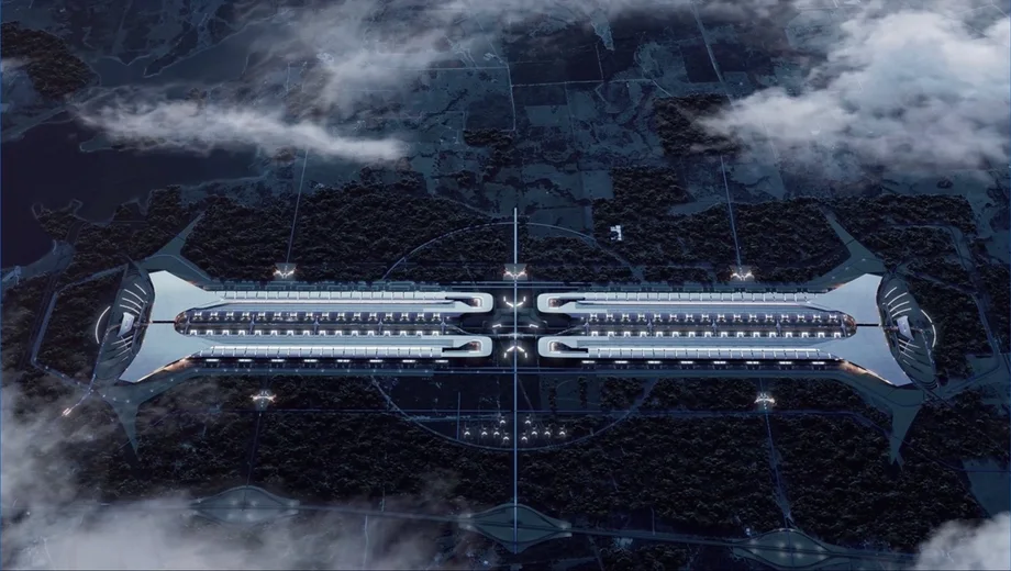
Austin is intended to serve as the proving ground before processes move to Grimes County. The larger project could eventually occupy a site of 100 million square feet. The immediate engineering milestone is much smaller: an SRAM test chip, a form of memory used to check whether the manufacturing process is functioning.
The dates that will measure progress
Musk's production schedule moves from a test chip in 2027 to volume manufacturing in 2028, followed by the much larger capacity ambition associated with 2032 and beyond. During SpaceX's October 20 earnings call, the Tesla and SpaceX chief described the dates this way:
very aggressive
The main milestones and spending announcements are:
- March 2026: Tesla and SpaceX announced the Terafab concept.
- April 2026: Intel announced cooperation on design, manufacturing and packaging.
- August 6, 2026: Abbott's office estimated the Gibbons Creek first phase at more than $16.8 billion.
- October 20, 2026: Musk outlined the test chip and volume production targets during SpaceX's earnings call.
- November 6, 2026: Musk accepted $1 trillion as a possible eventual cost at the Baron Investment Conference.
- May or June 2027: Target for the first SRAM test chip.
- Third quarter of 2028: Target for volume production.
- 2032 or later: Period associated with the proposed capacity of 1 million wafers a month.
The 2028 production target covers the start of manufacturing at volume. The million wafer ambition represents a later expansion requiring further equipment, construction and investment.
A terawatt of chips is a separate ambition
Musk has also framed Terafab's goal as producing AI chips each year with a combined power rating of 1 terawatt, or 1,000 gigawatts. At the November 6 Baron Investment Conference, he described the scale of that goal:
terrifyingly large
The power figure describes the intended annual output of chips in terms of the electricity they would use when operating. Wafer capacity measures how much silicon a factory can process. Connecting the two requires details about chip designs, power consumption and production yield.
Musk estimated worldwide AI chip output at around 20 to 25 gigawatts in 2026 and 35 to 45 gigawatts in 2027. Against his 2027 range, 1,000 gigawatts works out to roughly 22 to 29 times global production. His description of about 30 times is a rounded comparison.
SpaceX is already a large buyer of computing hardware. Musk said it purchases roughly 200,000 Nvidia GB300s a month. Terafab would create an internal manufacturing operation alongside that reliance on outside suppliers, serving plans that include computing infrastructure in orbit.
Musk has also argued that manufacturing is too concentrated in Asia. He estimated that even after counting all announced American factory projects, US capacity would be about one tenth of Asia's. That concern helps explain why the venture is centered in Texas despite the scale of equipment and expertise it must secure internationally.
Who will fund the expansion?
Investor Ron Baron raised the $1 trillion figure at the November 6 conference. Musk accepted it as a possible cost over time and said spending would happen in phases. An earlier estimate had placed total spending above $100 billion, while Abbott's office identified more than $16.8 billion for the first phase alone.
Texas plans to support Terafab with a $30 million Texas Enterprise Fund grant and tax incentives through its Jobs, Energy, Technology and Innovation program. The grant equals about 0.18% of $16.8 billion, leaving the companies and any financing partners responsible for nearly all of the capital requirement.
Tesla and SpaceX face other large spending demands. Tesla's third quarter free cash flow fell 61.63% as capital expenditure rose 110.5%. SpaceX reported $4.40 billion in quarterly earnings and projected fourth quarter capital expenditure of $35 billion to $40 billion.
The proposed SpaceX–Tesla combination adds another unresolved decision. Independent committees examining a merger have not agreed on terms, leaving responsibility for Terafab's later funding unsettled. Raising money through new shares would spread ownership across more shares and reduce existing investors' percentage stakes.
For Texas, the next concrete tests are equipment arrival, successful test chips and the transition to production. For Tesla and SpaceX, the larger challenge is turning a phased construction plan into a reliable source of memory and logic chips while funding their other businesses.
Key Points
- Terafab has outlined capacity of 1 million wafers a month, split between 700,000 for memory and 300,000 for logic.
- The memory target approaches Samsung's cited DRAM capacity of 650,000 to 700,000 wafers a month.
- The first Texas phase is estimated at more than $16.8 billion. Musk has accepted that spending could eventually reach $1 trillion.
- The first SRAM test chip is targeted for May or June 2027, followed by volume production in the third quarter of 2028.
- Intel is cooperating on manufacturing technology. TSMC participation and a memory technology partner remain unsettled.
- Equipment availability, reliable production and financing will determine how quickly the venture can expand toward its longer term target.