
Five operating plants do not mean five wafer fabs
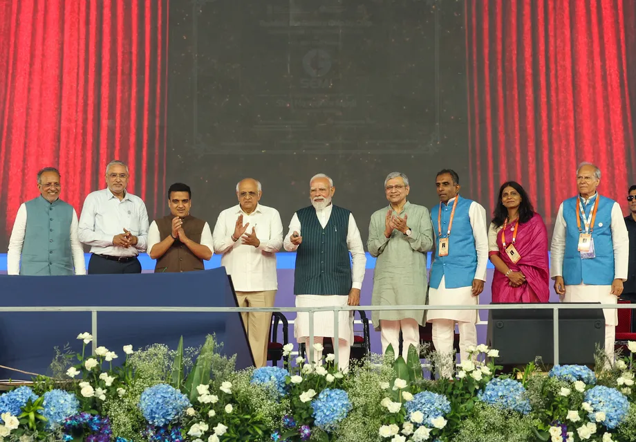
India's semiconductor expansion has reached commercial production, but its first operating plants are concentrated in packaging and testing rather than the fabrication of silicon chips. At SEMICON India in New Delhi on 17 September 2026, Prime Minister Narendra Modi celebrated five operating semiconductor plants. The distinction matters: these facilities assemble, connect, protect and test chips, rather than manufacture their electronic circuits on silicon wafers.
Contents
- Five operating plants do not mean five wafer fabs
- A broad programme with a packaging led start
- What the production timeline actually shows
- Sanand moves from testing to commercial shipments
- Tata's Assam plant and Gujarat fab do different jobs
- Moving beyond China does not mean making everything locally
- Odisha's glass project raises the technical stakes
- Workers and equipment support must grow with the plants
- The next phase needs measurable domestic value
- Key Points
The five operating units should also be distinguished from five prominent investment ventures often grouped together in accounts of India's packaging industry. A report on the September summit identified CDIL Semiconductor's assembly, testing, marking and packaging facility and Suchi Semicon's outsourced assembly and test facility as the two latest commercial additions. Electronics and IT Secretary S Krishnan confirmed the operating count of five. Other major projects, including Tata Electronics' Assam plant and the HCL and Foxconn venture in Uttar Pradesh, were still at different stages of development.
That makes India's progress real, but narrower than a headline about five chip plants might suggest. Outsourced semiconductor assembly and test, known as OSAT, is part of semiconductor manufacturing. It is not the same as wafer fabrication, which creates the microscopic circuits that perform a chip's calculations, store information or control electrical power.
The distinction does not make packaging a minor business. India's projects range from conventional assembly to automotive modules and advanced three dimensional integration. The central question is how much technical capability and domestic economic value these plants can build while fabrication projects, suppliers and skilled workers catch up.
A broad programme with a packaging led start
The India Semiconductor Mission's Semicon India programme records that the Union Cabinet approved an outlay of INR 76,000 crore in 2021. Its scope includes silicon and display fabrication, semiconductor design, packaging, compound semiconductors, silicon photonics and sensors. Packaging is therefore one supported route into the industry, not the programme's final destination.
The government's mission overview describes the same commitment as approximately $10 billion. It also cites a proposed $10 billion fabrication project in Maharashtra with expected capacity of 80,000 wafers a month, and says NXP Semiconductors is investing more than $1 billion in India in areas including automotive electronics and telecommunications. Those statements describe investment ambitions, not evidence that the proposed wafer capacity is operating.
The overview projects an Indian semiconductor market worth $63 billion by 2026. That is a market forecast, not a measure of domestic chip production. Demand for semiconductors can grow while the circuits inside packaged products continue to arrive from overseas.
Dates and project counts require similar care. The official programme page lists SEMICON India 2025 for 2–4 September at Yashobhoomi in New Delhi. The September 17 announcement belongs to the reported 2026 event, held on 17–19 September at the same venue. Accounts also describe ten approved projects across six states in one period and nearly 12 by October 2026. Approval, pilot production and commercial operation are separate milestones.
What the production timeline actually shows
Several developments help explain how India reached the five plant announcement. They also show why an inauguration date is not always the date when equipment first begins testing chips.
- 2021: The Union Cabinet approved the INR 76,000 crore Semicon India programme.
- 2024: The foundation stone was laid for CG Semi's Sanand facility in Gujarat.
- August 2025: CG Semi began chip testing, according to the Prime Minister's Office.
- February and March 2026: Reports describe Micron's Sanand inauguration in February and Kaynes Semicon's Sanand inauguration in March.
- 4 July 2026: Modi inaugurated CG Semi's OSAT facility, with commercial packaging underway.
- 17–19 September 2026: SEMICON India took place in New Delhi, with five operating units reported.
- 3 October: Assam Chief Minister Himanta Biswa Sarma said Tata's first Jagiroad clean room was ready and pilot chip production had begun.
- December 2026 or January 2027: Tata's Assam facility is expected to be formally inaugurated.
- 2028: The HCL and Foxconn facility in Jewar is targeting operations.
The September summit reportedly drew more than 600 companies and 40,000 delegates from 52 countries, including 300 overseas firms. Infineon announced a 28% expansion of its workforce in India. These are signs of commercial interest, but neither conference attendance nor hiring announcements establish how much qualified production a plant can deliver.
Descriptions of a third facility also differ. The Prime Minister's Office called CG Semi the third major facility in July, while a separate account described Tata's planned Assam unit as India's third OSAT facility. The accounts do not establish a common counting method, so those labels cannot be treated as a single consistent operating sequence.
Sanand moves from testing to commercial shipments
The Prime Minister's Office's CG Semi inauguration statement, dated 4 July 2026, says commercial chip packaging had commenced at the Sanand facility. It gives annual production capacity of 20 crore units, or 200 million, and a target of 500 crore units, or five billion. The target is 25 times the stated initial annual capacity.
Modi, speaking as prime minister at the inauguration, described an ambition extending beyond packaging.
Our goal is to build a complete semiconductor ecosystem in India, from chip design to fabrication and packaging.
CG Semi's INR 7,600 crore venture brings together CG Power, Japan's Renesas Electronics and Thailand's Stars Microelectronics. Its reported focus includes automotive microcontrollers, which manage functions inside vehicles. Renesas contributes semiconductor expertise, while Stars provides packaging technology and training support.
Capacity figures differ between accounts. Reporting describes a target of 15 million units a day and a second expansion phase targeting 14.5 million units a day by the end of 2026. These figures do not directly match the government's annual figures. Without a shared definition of operating days, plant phases and product mix, they should not be combined into a single capacity estimate.
Sanand also hosts Micron's $2.75 billion assembly, testing, marking and packaging plant. Reports say its more than 500,000 square feet of clean room space supported commercial shipments to Dell and HP within weeks of opening. Kaynes Semicon's INR 3,307 crore plant targets about 6.33 million chips a day. It acquired Fujitsu power module production lines for $13.8 million in June 2025 and is working with IBM on flip chip and three dimensional packaging research.
Tata's Assam plant and Gujarat fab do different jobs
Tata Electronics' INR 27,000 crore Jagiroad project in Assam is designed for up to 48 million semiconductor units a day. Its first clean room and pilot activity mark progress toward commercial production, but pilot output does not establish that the plant has reached its planned volume.
One account expected production to start in December without specifying a year. A later account placed formal inauguration in December 2026 or January 2027 after the October pilot announcement. These milestones need not conflict: pilot assembly, commercial production and a formal opening can occur at different times. A confirmed commercial start date and achieved output remain distinct from the inauguration forecast.
Jagiroad will use wire bond, flip chip and Integrated Systems Packaging technologies. Wire bonding connects a chip to its package with fine wires. Flip chip technology connects it through contacts on its face. Both make a fabricated chip usable within a larger electronic product.
Tata and Qualcomm Technologies plan to manufacture Qualcomm Automotive Modules at Jagiroad for Indian and global automakers. These combine Snapdragon Digital Chassis chips with other components for digital cockpits, infotainment, connectivity and intelligent vehicle systems. Tata also plans to assemble and test Nexperia's discrete semiconductor products there, meaning devices that perform individual electrical functions.
Tata's Dholera project in Gujarat has a different role: it is an upcoming 300mm wafer fabrication plant, with Taiwan's PSMC as a process technology partner and ASML supplying lithography equipment. Tata and Nexperia are preparing for production of Nexperia's MOSFET portfolio there. MOSFETs are transistors commonly used to switch or control electrical power. Packaging Nexperia products in Assam and fabricating them in Gujarat would represent two different stages of the production chain.
Moving beyond China does not mean making everything locally
India's emerging packaging ventures are building supplier networks outside China. Reports estimate that typical OSAT supply chains draw 55–60% of their suppliers from China. That figure concerns supplier concentration, not necessarily China's share of each plant's purchasing expenditure.
Tata has reportedly signed at least nine suppliers outside China for Jagiroad, including Singapore's ASMPT, the Netherlands' Nexperia, Japan's Fujifilm and Malaysia's Kelington. The network covers equipment, materials and manufacturing support. Kaynes is working with Japan's AOI Electronics on packaging expertise and Mitsui & Co. on sourcing Japanese materials.
These choices seek to reduce exposure to export restrictions, tariff uncertainty and supply interruptions. They replace dependence on one geography with a broader international network, rather than remove import dependence.
Materials reportedly account for 45–50% of OSAT production expenses, with 60–70% still sourced internationally. Copper lead frames come largely from Korea and the Philippines. Bonding wire is supplied by firms including Japan's Tanaka Precious Metals and Germany's Heraeus Electronics. Epoxy moulding compounds, which protect packaged chips, arrive from Southeast Asia and require refrigerated transport.
Local projects could gradually change that balance. INOX Air Products is building purification facilities at Sanand and a specialist gas hub at Dholera. Linde has acquired land in Sanand, while HySpec Chemicals has committed INR 750 crore to semiconductor gases and chemicals. New suppliers usually need one to two years to qualify, and longer for automotive components. CG Semi estimates at least three years to build a local supply layer; the wider ecosystem has a reported development horizon of 10–15 years.
Odisha's glass project raises the technical stakes
The INR 1,934 crore project led by US based 3D Glass Solutions in Bhubaneswar shows why packaging should not be treated as a single level of technology. Backed by investment from Intel, Lockheed Martin and other funds, it is intended to produce glass substrate panels and advanced three dimensional heterogeneous integration modules for artificial intelligence, 5G, defence and data centres.
Heterogeneous integration brings different kinds of chips, such as processors, memory and sensors, into one assembly. Three dimensional packaging can stack components vertically. A substrate supports and connects those components; glass offers potential advantages in stability, precision and signal performance. These methods seek better performance from the assembled system without relying only on making each individual transistor smaller.
Electronics and IT Secretary S Krishnan described the project as a distinctive part of the mission's first phase at its foundation ceremony.
Amongst all the ten projects that we have already approved under the India Semiconductor Mission, this is the one project which represents truly advanced packaging, this is technology which is new, which is novel,
Odisha Chief Minister Mohan Charan Majhi gave expected annual production figures of 70,000 glass panels and 50 million assembled units, and around 2,500 direct and indirect jobs. The account also cites about 13,000 advanced integration modules. Panels, assembled units and modules are different outputs and should not be added together.
The project remains a development commitment rather than demonstrated commercial capacity. Its importance lies in the kind of packaging India hopes to master, not simply in adding another factory to the national count.
Workers and equipment support must grow with the plants
New factories need experienced engineers alongside graduates, technicians and operators. Ashok Chandak, head of the India Electronics and Semiconductor Association, argues that education must translate into practical manufacturing skills.
The priority should be to build an industry-ready talent pipeline, not merely increase the number of graduates. Equally important is the need for skilled technicians, operators, and diploma-level talent who will form the backbone of manufacturing operations,
The workforce requirement extends to component suppliers, specialist chemical and gas facilities, and logistics. Recruiting experienced engineers of Indian origin from overseas could help new teams learn production processes while colleges and training institutions build a sustained supply of workers.
At CG Semi's inauguration, Modi described young women from tribal communities who had progressed from industrial training institutes to technical training in Malaysia. That example illustrates how operating skills can be developed through international partnerships.
Equipment maintenance is another part of the emerging industry. Canon India President and CEO Toshiaki Nomura said the company had discussed projects with key manufacturers and planned local support for its lithography technology. Lithography transfers circuit patterns onto wafers during fabrication.
Nomura explained that dedicated service infrastructure would follow confirmed projects.
Once the project is confirmed, of course we need 24x7 support to the chip manufacturer. In that sense, we will bring our technologies and service centres in India. That's our plan,
Those discussions are not confirmed equipment orders. They nevertheless show that establishing fabrication requires maintenance and technical support alongside the machines themselves.
The next phase needs measurable domestic value
Rakesh Kumar, a University of Illinois professor and author of The Chip Age, argues that India should prioritise packaging, testing, design and legacy chip manufacturing in the medium term. Legacy chips use established production technologies and remain relevant to sectors such as automotive electronics.
Kumar describes China's experience as both an example of sustained investment and a warning about dependence on foreign equipment.
China serves both as a good role model as well as a cautionary tale,
His argument is that spending alone cannot guarantee access to advanced technology when export controls can interrupt essential supplies. He recommends a commitment of 10–20 years to legacy manufacturing, supported by domestic demand and policies such as preferential access and tariffs. He also argues for strong Indian chip design companies that can compete as artificial intelligence changes design work.
For public subsidies, Kumar proposes weighing local value added, employment, tax revenue and security benefits. His hypothetical example of a $3 billion foundry requiring $2.5 billion in government support illustrates that tradeoff; it is not an announced Indian project.
The next mission phase is described differently across reports. One cites a budget of INR 1.27 lakh crore, while another describes a possible programme of approximately $11 billion. These figures cannot be presented as a single confirmed allocation. Krishnan's reported priorities include design, packaging, testing, materials and supply integration.
The next concrete milestones include CG Semi's expansion target by the end of 2026, Tata's expected Assam inauguration in December 2026 or January 2027, and the Jewar project's 2028 operating target with planned capacity of 20,000 wafers a month. Actual commercial output, supplier qualification and progress at fabrication projects will provide a more useful measure of India's capabilities than factory counts alone.
Key Points
- India's five operating semiconductor plants announced in September 2026 were concentrated in assembly, packaging and testing, not large scale wafer fabrication.
- The INR 76,000 crore programme approved in 2021 supports fabrication, packaging, design and other semiconductor technologies.
- CG Semi, Micron and Kaynes have advanced production in Sanand, while Tata's Assam project has entered pilot activity.
- Tata's Jagiroad packaging plant and Dholera wafer fab perform different stages of semiconductor manufacturing.
- Supplier diversification beyond China reduces geographic concentration but leaves substantial reliance on imported materials and equipment.
- Odisha's glass substrate project aims to establish advanced packaging capabilities, with commercial performance still to be demonstrated.
- Skilled workers, qualified suppliers and measurable domestic value will determine how far operating plants translate into a broader semiconductor industry.