

A Chinese chipmaker enters Nvidia's power plans
Innoscience, founded in 2015 by former NASA scientist Dr. Luo Weiwei, has reached a new stage in its expansion: Nvidia named the company in August 2025 as its sole Chinese supplier for the advanced 800 VDC power architecture planned for its next generation of AI data centers. As of August 29, the collaboration remained in testing, with no formal orders yet placed.
Contents
- A Chinese chipmaker enters Nvidia's power plans
- From NASA to a company in Zhuhai
- Why gallium nitride matters
- Larger wafers and control of production
- What the Nvidia connection involves
- Chinese suppliers and an international alliance
- The milestones behind the expansion
- Patent disputes cross several borders
- Market leadership has yet to deliver profits
- Luo's proposed chip era for power electronics
- A Chinese ambition with global connections
- Key Points
The opportunity brings together several parts of Innoscience's story. The company has become the world's largest dedicated manufacturer of gallium nitride power devices, built manufacturing operations in Zhuhai and Suzhou, and raised HK$1.4 billion through a Hong Kong listing in December 2024. Its chips address a growing problem for AI computing: supplying large amounts of electricity efficiently.
Gallium nitride, usually shortened to GaN, is a semiconductor material used to control electrical power. Innoscience's role concerns the power supplied to computing equipment. Its third generation of GaN devices covers voltages from 15 V to 1200 V, giving the company products for different stages of a power supply system.
Luo's business also faces substantial pressures. Innoscience remains unprofitable, is involved in patent disputes with overseas competitors, and has reportedly quoted prices around half those of other global GaN companies. Its expansion is taking place while the United States and China pull apart in advanced chip technology and China seeks greater independence in semiconductor production.
The result is a company with growing manufacturing scale and international connections, but with commercial, financial and legal challenges still to resolve. Nvidia's testing is one opportunity within that wider business.
From NASA to a company in Zhuhai
Luo holds a doctorate in applied mathematics from Massey University and spent 15 years at NASA, working on aerospace technologies and building her scientific career. She returned to China in 2015 and founded Innoscience in Zhuhai.
Her decision combined a business strategy with a patriotic ambition: building a Chinese leader in power electronics by investing in GaN. As the United States tightened restrictions on chip exports to China, domestic semiconductor development became increasingly important to China's technology plans.
Luo now serves as Innoscience's chairperson. Through various shareholding arrangements, she controls more than a third of the company's equity, giving her a substantial ownership position alongside her leadership role.
Her chosen field is power electronics, the technology that controls and converts electricity so equipment receives the power it needs. Innoscience's products serve consumer electronics, wind power, industrial automation, automotive electronics and AI data centers. The common requirement across those applications is managing electricity efficiently in a limited amount of space.
Why gallium nitride matters
GaN belongs to a group of materials known as wide bandgap semiconductors. Compared with traditional silicon, it can operate at higher voltages, frequencies and temperatures. Those properties make it useful where equipment needs both efficient power conversion and high power density, meaning more power handled within a smaller space.
Power devices repeatedly switch electrical current on and off. Some energy is lost during those changes. GaN's advantages over silicon include up to 15 times lower losses when switching off and three times lower losses when switching on. Higher switching frequencies also allow smaller and lighter systems.
Those benefits matter in AI data centers, electric vehicles and renewable energy systems, where electrical efficiency and equipment size affect system design. Lower energy consumption can also reduce associated carbon dioxide emissions.
Luo, speaking as Innoscience's chairperson at the IPF 2025 Conference, described the practical purpose of the technology:
GaN technology is essential to improve electronics, creating smaller and more efficient systems which save electric power, lower cost, and reduce CO2 emissions.
Innoscience's strategy connects those material advantages with manufacturing changes. More compact designs can support automated production and more standardized performance, bringing power electronics closer to the repeatable production methods used elsewhere in the chip industry.
Larger wafers and control of production
Innoscience's central manufacturing achievement is mass production of GaN devices on silicon wafers measuring 8 inches across. Wafers are the surfaces on which semiconductor devices are manufactured. A larger wafer provides more space for production.
Compared with the industry standard of 6 inches, Innoscience's move to wafers measuring 8 inches increased chip output by 80% and reduced unit costs by 30%. The company became the only producer globally capable of manufacturing GaN products across a full voltage spectrum at industrial scale.
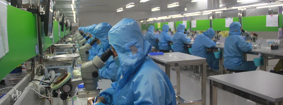
Innoscience operates as an integrated device manufacturer, or IDM. It controls chip design, wafer manufacturing, packaging and reliability testing. Packaging prepares a chip for use in electronic equipment, while reliability testing checks whether it can perform consistently.
Keeping those stages within one company supports faster development, high manufacturing yields and greater resilience when supply chains are disrupted. Yield describes the share of production that meets the required standard. Innoscience's yield exceeded 95% by late 2024.
By 2024, the company's monthly GaN wafer production capacity had reached 13,000 wafers, supported by its production bases in Suzhou and Zhuhai. Capacity describes how much a manufacturer can produce, while the yield figure describes how successfully that production meets specifications. Together, the figures show the scale and manufacturing performance behind Innoscience's expansion.
What the Nvidia connection involves
Nvidia's planned 800 VDC architecture uses direct current, the form of electricity indicated by DC. Innoscience's selection places its power devices within the development of an advanced electricity supply system for the next generation of AI data centers.
Nvidia is a bellwether for the AI hardware industry, so its selection of Innoscience drew attention beyond the immediate testing work. Innoscience's third generation of GaN devices provides a comprehensive power supply solution covering 15 V to 1200 V.
For Innoscience, the opportunity combines a demanding application with a globally important potential customer. AI data centers are a particular focus of the company's expansion because demand for efficient chips capable of handling high power is rising.
The relationship also connects with Innoscience's legal disputes. Infineon Technologies, another key Nvidia partner, has brought patent cases against the Chinese company. Innoscience is therefore pursuing a place in Nvidia's future power systems while contesting intellectual property claims from another participant in that business.
Chinese suppliers and an international alliance
Innoscience's supply chain includes JCET for chip packaging, San'an Optoelectronics for high purity sapphire substrates, and Naura Technology for MOCVD equipment. MOCVD equipment is essential for GaN epitaxy, the process used to grow the semiconductor layers needed for devices.
Those relationships illustrate the growing range of capabilities within China's semiconductor industry. Packaging, materials and manufacturing equipment are different parts of chip production, and Innoscience's network brings Chinese companies into each of those activities.
International cooperation remains part of the business. In April 2025, Innoscience signed an agreement with STMicroelectronics, known as ST, allowing both companies to use each other's GaN wafer manufacturing capacity. The arrangement aims to accelerate GaN adoption worldwide and give customers more flexibility in their supply chains.
Luo, commenting as Innoscience's chairperson on the STMicroelectronics agreement, said:
The joint collaboration between ST and Innoscience will further expand and accelerate the adoption of GaN technology. Together the teams at Innoscience and ST will develop the next generations of GaN technology.
Innoscience began international operations in the United States and Europe in 2022. Another potential change in the competitive market is Taiwan Semiconductor Manufacturing Company's plan to leave the GaN wafer foundry business by 2027. A foundry manufactures chips for other businesses. TSMC's planned withdrawal is expected to strengthen Innoscience's market position.
The milestones behind the expansion
Innoscience's growth has involved factory development, international expansion, legal proceedings and access to public investment. The main dates show how those activities have developed alongside one another.
- 2015: Luo returned to China and founded Innoscience in Zhuhai after spending 15 years at NASA.
- 2022: Innoscience began international operations in the United States and Europe.
- July 2023: The United States International Trade Commission investigated Innoscience following a patent complaint by Efficient Power Conversion.
- November 2024: The commission ruled that Innoscience had infringed an EPC patent and issued a limited exclusion order covering certain chip imports.
- December 2024: Innoscience listed on the Hong Kong Stock Exchange, raising HK$1.4 billion at a valuation of HK$27 billion.
- March 2025: Innoscience secured a legal victory when the Patent Trial and Appeal Board invalidated EPC's claims.
- April 2025: Innoscience and STMicroelectronics signed their manufacturing capacity agreement.
- August 2025: Nvidia named Innoscience as its sole Chinese supplier for its advanced 800 VDC power architecture.
- 2027: TSMC plans to exit the GaN wafer foundry business.
The sequence places the Nvidia development within a longer expansion. Innoscience had already entered overseas markets, completed its public listing and agreed to share manufacturing capacity with ST before the August announcement.
Patent disputes cross several borders
Efficient Power Conversion, known as EPC, brought the complaint that led to the US International Trade Commission investigation in July 2023. The commission's November 2024 ruling found infringement of an EPC patent and imposed a limited exclusion order on certain chip imports.
Innoscience appealed. In March 2025, the Patent Trial and Appeal Board invalidated EPC's claims, giving the company a legal victory as it continued to pursue international business.
Infineon Technologies has also initiated a series of patent infringement lawsuits against Innoscience in the United States and Germany. Innoscience has countersued in China. The disputes place the company's technology and access to overseas markets within legal proceedings across several jurisdictions.
For a manufacturer seeking customers around the world, patents are part of the commercial competition alongside performance, price and production capacity. Innoscience's disputes have developed during the same period as its overseas expansion and its efforts to secure roles in major power electronics applications.
Market leadership has yet to deliver profits
Innoscience ranked first by revenue in the global GaN power device market in 2023, with a market share of 33.7%. It held a leading share of 29.9% in 2024. The two figures show a decline of 3.8 percentage points between those years while the company retained its leading position.
Revenue rose from RMB 68 million in 2021 to RMB 593 million in 2023. That was an increase of RMB 525 million, with 2023 revenue about 8.7 times the 2021 figure. The growth illustrates the speed at which sales expanded as Innoscience developed its production and customer base.
Net losses nevertheless persisted. Heavy research and development spending, continuing investment in capacity and technology, and aggressive pricing have weighed on profitability. Innoscience's reported price quotations of about half those of other global GaN companies have also raised concerns about a potential price war and its effects on the industry.
The December 2024 initial public offering brought Innoscience HK$1.4 billion and a valuation of HK$27 billion. Major investors include China Merchants Bank, Wujiang Industrial Investment, South Korea's SK Inc. and several state backed funds.
That investor group combines Chinese and international capital. The listing gave public investors access to a company with rapidly growing revenue and substantial manufacturing capacity, alongside continuing losses and the costs of developing new technology.
Luo's proposed chip era for power electronics
Luo's wider ambition is to change how power electronics are made. Her vision of a "Chip Era" involves moving from manual assembly toward automation and replacing fragmented solutions with standardized manufacturing guided by science.
GaN's smaller system designs are central to that approach. Integrating passive components onto printed circuit boards and using automated production can deliver more predictable performance, lower costs and greater reliability. The aim is to make production more consistent as well as making individual devices more efficient.
Luo described that vision at the IPF 2025 Conference:
GaN allows the industry to move from craftsmanship to science, from manual assembly to automation, and from fragmentation to standardization, marking the arrival of the chip era for power electronics.
AI servers, electric vehicles and robotics are among the sectors where GaN's efficiency and power density are opening possibilities. Innoscience's strategy brings those applications together with its larger wafers, integrated manufacturing model and broad range of operating voltages.
A Chinese ambition with global connections
China is investing heavily in domestic innovation and manufacturing as geopolitical tensions and export controls disrupt global supply chains. Innoscience's development in GaN, a field traditionally led by the United States and Europe, shows how a Chinese manufacturer is seeking leadership in a strategic technology.
Its operations also show how domestic independence and international business can develop together. Chinese suppliers support its production network, while STMicroelectronics provides a manufacturing alliance, overseas investors hold stakes, and Nvidia's power architecture presents a potential commercial opportunity.
The global GaN power device market is projected to reach US$4.376 billion by 2030, with a compound annual growth rate of nearly 50%. Compound growth means each year's increase builds on the previous year's larger market. Such a forecast points to rapidly expanding demand for efficient power devices.
As of August 29, 2025, Innoscience's position combined manufacturing leadership, a growing international presence and unresolved business pressures. Turning its production scale and technical range into profitable sales is the central commercial task as it pursues Luo's vision for power electronics.
Key Points
- Luo Weiwei founded Innoscience in Zhuhai in 2015 after a scientific career that included 15 years at NASA.
- Nvidia named Innoscience its sole Chinese supplier for an advanced 800 VDC architecture in August 2025; testing continued without formal orders.
- Innoscience's wafers measuring 8 inches increased chip output by 80% and reduced unit costs by 30% compared with wafers measuring 6 inches.
- Monthly GaN wafer production capacity reached 13,000 in 2024, and manufacturing yield exceeded 95% by late that year.
- The company raised HK$1.4 billion in its December 2024 Hong Kong listing but remained unprofitable.
- STMicroelectronics signed a manufacturing capacity agreement with Innoscience in April 2025.
- Patent disputes involving EPC and Infineon have accompanied Innoscience's international expansion.
- The global GaN power device market is projected to reach US$4.376 billion by 2030.