

A 2030 start, followed by a larger mask transition
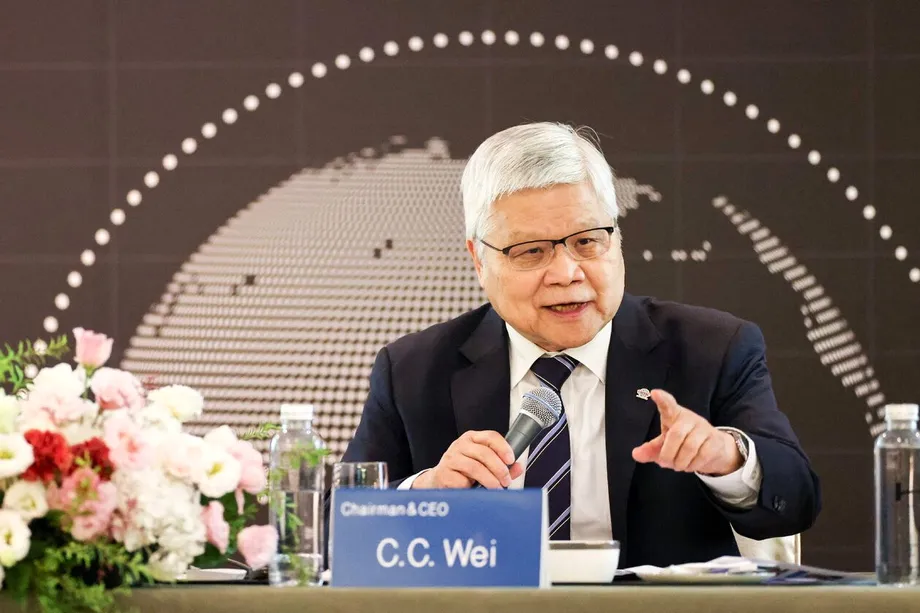
TSMC plans to begin using ASML's High-NA EUV lithography technology in advanced chip mass production in 2030, choosing to wait for better manufacturing readiness and more suitable costs even as Intel gains experience with the equipment. Chairman and CEO C.C. Wei says the later start will not put the Taiwanese chipmaker at a competitive disadvantage.
Contents
- A 2030 start, followed by a larger mask transition
- Why TSMC is waiting for manufacturing readiness
- What High-NA changes inside a chip factory
- Why larger photomasks matter
- The milestones through 2033
- Intel and Samsung are moving earlier
- A14 demand is growing before High-NA arrives
- Packaging is expanding alongside finer circuits
- Capacity and spending follow customer needs
- Key Points
The timetable has two stages. TSMC will initially use existing 6-inch photomasks, which carry the circuit patterns transferred onto silicon wafers. A joint industry initiative with ASML targets a pilot line for larger, 12-inch masks by 2031, followed by lithography systems ready to support advanced chip production by 2033.
ASML and TSMC set out those milestones in their September 8, 2026, joint technology announcement. The companies said they formed the initiative a day earlier, ahead of the SPIE BACUS conference in Monterey, California. Their stated goals are greater factory productivity, lower chipmaking costs and fewer restrictions when printing large circuit patterns.
Wei reaffirmed the 2030 adoption plan during TSMC's third quarter investor discussion. His position ties the purchase and use of a powerful new tool to the practical demands of producing chips reliably and at a price customers can support.
Why TSMC is waiting for manufacturing readiness
Wei described three requirements for bringing new equipment into mass production: technical capability, reasonable cost and maturity. He placed the greatest weight on maturity, meaning the equipment and its supporting manufacturing processes must be ready for dependable use across large production volumes.
TSMC expects High-NA EUV to meet those conditions more comfortably in 2030. The company is improving production efficiency and working closely with ASML while continuing to develop advanced processes using its existing lithography technology.
High-NA exposure machines have been described as costing about US$400 million each. At that price, the business decision extends beyond how small a pattern the equipment can print. TSMC must also consider how many wafers it can process, how consistently it operates and how many usable chips emerge from production.
A usable chip matters more to a customer than a successfully completed exposure step. A more expensive machine can still make economic sense if it removes other manufacturing steps or raises output. Wei's timetable rests on the expectation that the combined technical and financial conditions will become suitable for TSMC's production needs by 2030.
What High-NA changes inside a chip factory
Lithography uses light to transfer circuit patterns onto a coated silicon wafer. Chipmakers repeat this and other manufacturing steps to build the many layers that make a processor work. EUV stands for extreme ultraviolet, the type of light used to create exceptionally fine patterns.
High-NA improves the optical system. Numerical aperture, shortened to NA, describes its ability to collect light and resolve fine detail. Current EUV systems have an NA of 0.33; High-NA raises that figure to 0.55.
The stated minimum resolution improves from about 13 nanometres to 8 nanometres in a single exposure. That is a reduction of roughly 38% in the smallest resolved dimension, calculated from those two figures. For some patterns, the finer resolution could replace two or more exposures with one, reducing manufacturing steps, production time and opportunities for defects.
The optical change also creates a constraint: with existing masks, High-NA exposes an area about half the size of a conventional EUV exposure field. A large chip pattern may therefore require separate exposures joined through a process called stitching. That makes mask size an important part of the transition, especially for large processors used in artificial intelligence.
Why larger photomasks matter
TSMC and ASML plan to move from the current mask format, approximately 6 by 6 inches, toward a larger format described as 12-inch masks, approximately 6 by 12 inches. These measurements refer to the patterned masks used by lithography equipment. Silicon wafers are the separate discs on which the chips are manufactured.
The companies expect larger masks to increase scanner productivity, reduce chipmaking costs and remove stitching constraints. A scanner is the lithography machine that projects the mask's pattern onto the wafer. Its productivity affects how much manufacturing work a factory can complete with expensive equipment.
ASML president and CEO Christophe Fouquet explained the planned sequence in the joint announcement:
We expect the adoption of High NA EUV to increase progressively along the device scaling roadmap, first using current 6-inch masks and then further supported by 12-inch masks, which enable greater scanner productivity and allow the industry to meet the demand for smaller, faster and more energy-efficient chips.
The transition requires work beyond the scanner itself. Mask production, writing tools, handling equipment and design software must support the larger format. TSMC's initial 2030 production plan uses the established mask size, with the larger format following as the supporting systems become ready.
The milestones through 2033
TSMC's schedule separates the first use of High-NA in mass production from the later introduction of larger masks. The joint announcement gives three manufacturing targets, while the company's process roadmap places several chip generations before them.
- 2025: TSMC's N2 process entered mass production in the fourth quarter.
- 2027: A14 is expected to begin trial production.
- 2028: A14 is scheduled for mass production.
- 2029: A13 and A12 are expected to reach mass production using existing EUV technology.
- 2030: TSMC intends to begin High-NA EUV mass production for advanced nodes with current 6-inch masks.
- 2031: The ASML and TSMC initiative targets a pilot line for 12-inch photomasks.
- 2033: The initiative targets lithography system readiness for advanced chip production using the larger masks.
The September announcement presents the 2031 and 2033 dates as targets. A pilot line allows companies to develop and refine a manufacturing approach before wider production. Full system readiness requires the equipment and supporting processes to work together.
TSMC has not disclosed the first process node that will use High-NA in 2030, the number of machines it plans to deploy or the expected cost savings. A10 and A11 have attracted speculation as possible candidates, while A10 development has appeared in TSMC's research organisation. The company's formal adoption announcement leaves the first node unnamed.
Intel and Samsung are moving earlier
Intel assembled its first commercial High-NA EUV system in Oregon in 2024 and subsequently began using the technology for selected production layers. Intel and ASML have described applications involving Intel 18A and some Panther Lake processors sold under the Core Ultra Series 3 name.
By September 2026, Intel and ASML said more than 1 million wafers had been processed using High-NA equipment. That total covered equipment validation, testing, research and some production of specific product layers. Intel said selected 18A layers made with High-NA achieved performance at or above that obtained with existing 0.33 NA EUV.
Samsung has also announced plans to introduce High-NA EUV into DRAM mass production by 2028. DRAM is memory that temporarily holds information while a computer or other device is working. Samsung expects finer lithography to simplify parts of memory manufacturing and improve efficiency.
The companies are therefore pursuing different production schedules and applications. Intel is building operating experience on selected logic chip layers, Samsung is targeting memory, and TSMC is extending its current equipment strategy before starting High-NA production in 2030. All three have been identified as supporting the larger mask transition.
A14 demand is growing before High-NA arrives
TSMC's nearer term process plans are advancing on a separate schedule. Wei said the company is engaging with more customers on A14 than it did on N2 and expects A14 to become a larger node. A node is a generation of manufacturing technology with its own design rules, performance characteristics and production processes.
A14's planned 2028 production start comes two years before TSMC's intended High-NA introduction. A13, described as a refinement of A14, is expected to offer about 6% greater transistor density. A12 brings TSMC's Super Power Rail backside power technology to the A14 platform.
Backside power delivery routes electricity through the back of a chip, freeing space elsewhere for signal connections. Wei said adoption depends on the needs of each product: some AI accelerators may use it, while smartphone products may not.
Wei also said TSMC is preparing to increase production of small smartphone chips and much larger AI accelerators at the same time. He described the manufacturing learning curve as reasonable and said customers were satisfied. For customers, the immediate choice is among the processes and features suited to their products, with High-NA joining that set of manufacturing tools later.
Packaging is expanding alongside finer circuits
TSMC is also developing larger advanced packages that connect multiple chips and memory components. Wei said the company can mass produce products at five times reticle size, with strong yields, and is developing packages at nine times and eventually 14 times reticle size.
A reticle is a mask carrying a circuit pattern. In packaging discussions, multiples of reticle size describe the scale of the assembled package relative to a standard lithography field. Packaging connects components into a working system, while lithography creates patterns during chip manufacturing.
Wei said CoWoS remains the preferred packaging option for customers. TSMC is also developing CoPoS, a packaging approach using panels, to reduce future costs. Larger packages matter for AI systems because they allow processing chips and memory to be connected closely within a single assembly.
The official High-NA announcement links future demand for the equipment to increasingly complex transistor architectures used for AI applications. TSMC expects the number of layers requiring High-NA EUV to rise as its process generations advance. Its plan therefore combines finer chip manufacturing with larger and more capable packaging.
Capacity and spending follow customer needs
TSMC's capacity planning includes customers that design chips as well as companies that operate their own factories. Wei said the company treats both groups equally and takes a customer's internal manufacturing capacity into account when deciding how much production support to build.
Wei also said TSMC generally prohibits customers from reselling or auctioning their capacity allocations. Rare arrangements involving mask licensing cover very small wafer quantities. That policy gives TSMC a more direct role in deciding how its manufacturing capacity serves customer products.
Chief financial officer Wendell Huang said capital spending during 2026 to 2028 is expected to be substantially higher than in the preceding three years, although detailed figures for 2027 and later were still too early to provide. He said equipment, materials and labour costs were rising, with long term customer demand remaining the main driver of investment.
TSMC also expects overseas factory expansion to reduce gross margin by 3 to 4 percentage points in the later part of its five year planning period. Those spending pressures help explain why production efficiency features so heavily in the High-NA decision. A machine costing about US$400 million must fit a much larger plan for factory output, customer demand and profitability.
Wei described the purpose of the collaboration in the joint announcement:
We have always believed that when the industry works together to solve complex problems, we unlock possibilities that no single company could achieve alone,
TSMC's commitment is to begin High-NA production in 2030, then gain further productivity from larger masks as the industry completes the next stage of development. Customers will see the results through the manufacturing processes, available capacity and costs attached to their future chips.
Key Points
- TSMC intends to start High-NA EUV mass production for advanced nodes in 2030.
- Wei says technical maturity and reasonable cost guide the timing, and expects no competitive disadvantage from adopting later.
- Initial production will use existing 6-inch masks.
- TSMC and ASML target a larger mask pilot line by 2031 and supporting production system readiness by 2033.
- Intel has used High-NA for selected production layers; Samsung targets DRAM production by 2028.
- A14 is scheduled for mass production in 2028, ahead of TSMC's High-NA introduction.
- TSMC has yet to name its first High-NA process node or disclose equipment quantities and projected savings.